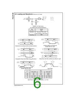
AC Loading and Waveforms Generic for LCX Family
FIGURE 1. AC Test Circuit
(CL includes probe and jig capacitance)
Test
Switch
Open
tPLH, tPHL
tPZL, tPLZ
6V at VCC = 3.3V ± 0.3V
CC x 2 at VCC = 2.5V ± 0.2V
GND
V
t
PZH, tPHZ
3-STATE Output Low Enable and
Waveform for Inverting and Non-Inverting Functions
Disable Times for Logic
Setup Time, Hold TIme and Recovery TIme for Logic
Propagation Delay, Pulse Width and trec Waveforms
3-STATE Output High Enable and
Disable Times for Logic
trise and tfall
VCC
Symbol
3.3V ± 0.3V
2.7V
1.5V
2.5V ± 0.2V
VCC/2
Vmi
Vmo
Vx
1.5V
1.5V
1.5V
VCC/2
VOL + 0.3V
V
OL + 0.3V
V
OL + 0.15V
Vy
V
OH − 0.3V
V
OH − 0.3V
VOH − 0.15V
FIGURE 2. Waveforms
(Input Pulse Characteristics; f = 1MHz, tr = tf = 3ns)
www.fairchildsemi.com
6

 FAIRCHILD [ FAIRCHILD SEMICONDUCTOR ]