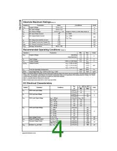
Absolute Maximum Ratings(Note 3)
Symbol
VCC
VI
Parameter
Supply Voltage
Value
Conditions
Units
V
−0.5 to +7.0
−0.5 to +7.0
DC Input Voltage
V
VO
DC Output Voltage
−0.5 to VCC + 0.5 Output in HIGH or LOW State (Note 4)
V
IIK
DC Input Diode Current
DC Output Diode Current
−50
−50
VI < GND
mA
IOK
V
V
O < GND
O > VCC
mA
+50
IO
DC Output Source/Sink Current
DC Supply Current per Supply Pin
DC Ground Current per Ground Pin
Storage Temperature
±50
mA
mA
mA
°C
ICC
±100
IGND
TSTG
±100
−65 to +150
Recommended Operating Conditions (Note 5)
Symbol
Parameter
Min
2.0
1.5
0.0
0.0
Max
3.6
Units
VCC
Supply Voltage
Operating
Data Retention
V
3.6
VI
Input Voltage
Output Voltage
Output Current
5.5
V
V
VO
HIGH or LOW State
VCC
±24.0
±12.0
±8.0
85.0
10.0
I
OH/IOL
V
V
V
CC = 3.0V to 3.6V
CC = 2.7V to 3.0V
CC = 2.3V to 2.7V
mA
TA
Free-Air Operating Temperature
−40.0
°C
∆t/∆V
Input Edge Rate, VIN = 0.8V to 2.0V, VCC = 3.0V
0.0
ns/V
Note 3: The Absolute Maximum Ratings are those values beyond which the safety of the device cannot be guaranteed. The device should not be operated
at these limits. The parametric values defined in the Electrical Characteristics tables are not guaranteed at the Absolute Maximum Ratings. The “Recom-
mended Operating Conditions” table will define the conditions for actual device operation.
Note 4: IO Absolute Maximum Rating must be observed.
Note 5: Unused inputs must be held HIGH or LOW. They may not float.
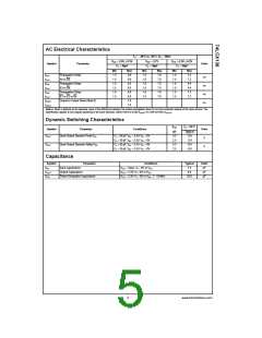
DC Electrical Characteristics
VCC
TA = −40°C to +85°C
Symbol
VIH
Parameter
Conditions
Units
(V)
2.3 to 2.7
2.7 to 3.6
2.3 to 2.7
2.7 to 3.6
2.3 to 3.6
2.3
Min
1.7
2.0
Max
HIGH Level Input Voltage
V
V
VIL
LOW Level Input Voltage
HIGH Level Output Voltage
0.7
0.8
VOH
I
OH = −100 µA
OH = -8 mA
OH = −12 mA
OH = −18 mA
OH = −24 mA
OL = 100 µA
IOL = 8mA
OL = 12 mA
OL = 16 mA
OL = 24 mA
0 ≤ VI ≤ 5.5V
V
CC − 0.2
1.8
I
I
2.7
2.2
V
V
I
3.0
2.4
I
3.0
2.2
VOL
LOW Level Output Voltage
I
2.3 to 3.6
2.3
0.2
0.6
I
2.7
0.4
I
3.0
0.4
I
3.0
0.55
±5.0
10.0
10.0
±10.0
500
II
Input Leakage Current
2.3 to 3.6
0.0
µA
µA
IOFF
ICC
Power-Off Leakage Current
Quiescent Supply Current
VI or VO = 5.5V
VI = VCC or GND
3.6V ≤ VI ≤ 5.5V
2.3 to 3.6
2.3 to 3.6
2.3 to 3.6
µA
µA
∆ICC
Increase in ICC per Input
VIH = VCC −0.6V
www.fairchildsemi.com
4

 FAIRCHILD [ FAIRCHILD SEMICONDUCTOR ]