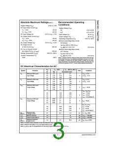
Absolute Maximum Ratings(Note 1)
Recommended Operating
Conditions
Supply Voltage (VCC
)
−0.5V to +7.0V
DC Input Diode Current (IIK
VI = −0.5V
)
Supply Voltage (VCC
)
−20 mA
+20 mA
AC
2.0V to 6.0V
4.5V to 5.5V
0V to VCC
VI = VCC + 0.5V
ACT
DC Input Voltage (VI)
−0.5V to VCC + 0.5V
Input Voltage (VI)
Output Voltage (VO)
DC Output Diode Current (IOK
)
0V to VCC
V
V
O = −0.5V
−20 mA
+20 mA
Operating Temperature (TA)
Minimum Input Edge Rate (∆V/∆t)
AC Devices
−40°C to +85°C
O = VCC + 0.5V
DC Output Voltage (VO)
DC Output Source
−0.5V to VCC + 0.5V
V
IN from 30% to 70% of VCC
or Sink Current (IO)
±50 mA
VCC @ 3.3V, 4.5V, 5.5V
Minimum Input Edge Rate (∆V/∆t)
ACT Devices
125 mV/ns
125 mV/ns
DC VCC or Ground Current
per Output Pin (ICC or IGND
)
±50 mA
Storage Temperature (TSTG
Junction Temperature (TJ)
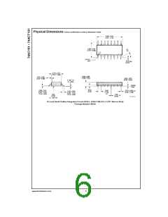
PDIP
)
−65°C to +150°C
V
IN from 0.8V to 2.0V
VCC @ 4.5V, 5.5V
140°C
Note 1: Absolute maximum ratings are those values beyond which damage
to the device may occur. The databook specifications should be met, with-
out exception, to ensure that the system design is reliable over its power
supply, temperature, and output/input loading variables. Fairchild does not
recommend operation of FACT circuits outside databook specifications.
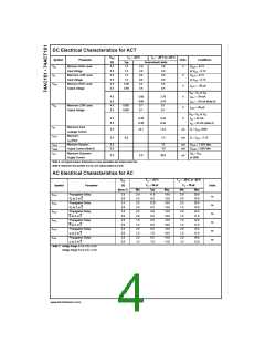
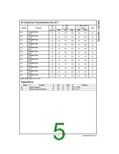
DC Electrical Characteristics for AC
VCC
T
A = +25°C
TA = −40°C to +85°C
Symbol
VIH
Parameter
Units
Conditions
(V)
3.0
4.5
5.5
3.0
4.5
5.5
3.0
4.5
5.5
Typ
1.5
Guaranteed Limits
Minimum HIGH Level
Input Voltage
2.1
3.15
3.85
0.9
2.1
3.15
3.85
0.9
V
OUT = 0.1V
2.25
2.75
1.5
V
or VCC − 0.1V
VIL
Maximum LOW Level
Input Voltage
V
OUT = 0.1V
2.25
2.75
2.99
4.49
5.49
1.35
1.65
2.9
1.35
1.65
2.9
V
V
or VCC − 0.1V
VOH
Minimum HIGH Level
Output Voltage
4.4
4.4
IOUT = −50 µA
5.4
5.4
V
IN = VIL or VIH
3.0
4.5
5.5
3.0
4.5
5.5
2.56
3.86
4.86
0.1
2.46
3.76
4.76
0.1
I
I
I
OH = −12 mA
V
V
OH = −24 mA
OH = −24 mA(Note 2)
VOL
Maximum LOW Level
Output Voltage
0.002
0.001
0.001
0.1
0.1
IOUT = 50 µA
0.1
0.1
V
IN = VIL or VIH
3.0
4.5
5.5
0.36
0.36
0.36
0.44
0.44
0.44
I
I
I
OL = 12 mA
V
OL = 24 mA
OL = 24 mA (Note 2)
IIN
(Note 4)
Maximum Input
Leakage Current
5.5
±0.1
±1.0
µA
V
I = VCC, GND
IOLD
IOHD
Minimum Dynamic
5.5
5.5
75
mA
mA
V
V
OLD = 1.65V Max
OHD = 3.85V Min
Output Current (Note 3)
−75
ICC
(Note 4)
Maximum Quiescent
Supply Current
5.5
4.0
40.0
µA
VIN = VCC or GND
Note 2: All outputs loaded; thresholds on input associated with output under test.
Note 3: Maximum test duration 2.0 ms, one output loaded at a time.
Note 4: IIN and ICC @ 3.0V are guaranteed to be less than or equal to the respective limit @ 5.5V VCC
.
3
www.fairchildsemi.com

 FAIRCHILD [ FAIRCHILD SEMICONDUCTOR ]