XRT86L30
REV. 1.0.1
SINGLE T1/E1/J1 FRAMER/LIU COMBO
When the Transmit Fractional DS1 bit of the Transmit Interface Control Register (TICR) is set to 1, this pin is
configured as TxSig_n pin, it acts as an input source for the signaling bits to be transmitted in the outbound
DS1 frames.
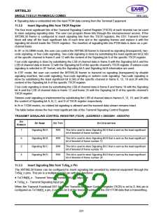
Figure 96 below is a timing diagram of the TxSig_n input pin. Please note that the Signaling Bit A of a certain
timeslot coincides with Bit 4 of the PCM data; Signaling Bit B coincides with Bit 5 of the PCM data; Signaling Bit
C coincides with Bit 6 of the PCM data and Signaling Bit D coincides with Bit 7 (LSB) of the PCM data.
FIGURE 96. TIMING DIAGRAM OF THE TXSIG_N INPUT
The table below shows configurations of the Transmit Fractional DS1 bit of the Transmit Interface Control
Register (TICR).
TRANSMIT INTERFACE CONTROL REGISTER (TICR)(ADDRESS = 0X0120H)
B
IT
B
IT
N
AME
B
IT
TYPE
BIT DESCRIPTION
N
UMBER
4
Transmit
R/W
This READ/WRITE bit-field permits the user to determine which one of the
two functions the multiplexed I/O pin of TxTSb[0]_n/TxSig_n is spotting.
Fractional DS1
0 - This pin is configured as TxTSb[0]_n pin, it outputs bit 0 of the timeslot
number of the DS1 PCM data that is transmitting.
1 - This pin is configured as TxSig_n pin, it acts as an input source for the
signaling bits to be transmitted in the outbound DS1 frames
222

 EXAR [ EXAR CORPORATION ]