XR-2206
With External Adjustment:
PRINCIPLES OF OPERATION
Description of Controls
Frequency of Operation:
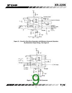
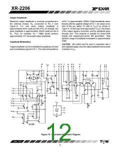
The harmonic content of sinusoidal output can be
reduced to -0.5% by additional adjustments as shown in
Figure 12. The potentiometer, R , adjusts the
A
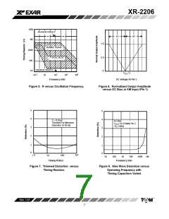
The frequency of oscillation, f , is determined by the
o
sine-shaping resistor, and R provides the fine
B
external timing capacitor, C, across Pin 5 and 6, and by
the timing resistor, R, connected to either Pin 7 or 8. The
frequency is given as:
adjustment for the waveform symmetry. The adjustment
procedure is as follows:
1. Set R at midpoint and adjust R for minimum
B
A
distortion.
1
RC
f0 +
Hz
2. With R set as above, adjust R to further reduce
A
B
distortion.
and can be adjusted by varying either R or C. The
recommended values of R, for a given frequency range,
as shown in Figure 5. Temperature stability is optimum
for 4kW < R < 200kW. Recommended values of C are from
1000pF to 100mF.
Triangle Wave Generation
The circuits of Figure 11 and Figure 12 can be converted
to triangle wave generation, by simply open-circuiting Pin
Frequency Sweep and Modulation:
13 and 14 (i.e., S open). Amplitude of the triangle is
Frequency of oscillation is proportional to the total timing
1
approximately twice the sine wave output.
current, I , drawn from Pin 7 or 8:
T
320IT (mA)
f +
Hz
FSK Generation
C(mF)
Figure 13 shows the circuit connection for sinusoidal FSK
signal operation. Mark and space frequencies can be
independently adjusted by the choice of timing resistors,
Timing terminals (Pin 7 or 8) are low-impedance points,
and are internally biased at +3V, with respect to Pin 12.
Frequency varies linearly with IT, over a wide range of
current values, from 1mA to 3mA. The frequency can be
R
1
and R ; the output is phase-continuous during
2
transitions. The keying signal is applied to Pin 9. The
circuit can be converted to split-supply operation by
simply replacing ground with V .
controlled by applying a control voltage, V , to the
activated timing pin as shown inFigure 10. Thefrequency
of oscillation is related to VC as:
C
-
VC
ǒ1 – Ǔ
3
1
RC
R
RC
f +
ǒ
1 )
Ǔ
Hz
Pulse and Ramp Generation
Figure 14 shows the circuit for pulse and ramp waveform
generation. In this mode of operation, the FSK keying
terminal (Pin 9) is shorted to the square-wave output (Pin
11), and the circuit automatically frequency-shift keys
itself between two separate frequencies during the
positive-going and negative-going output waveforms.
The pulse width and duty cycle can be adjusted from 1%
where V is in volts. The voltage-to-frequency conversion
gain, K, is given as:
C
0.32
RCC
K + ēfńēVC + –
HzńV
to 99% by the choice of R and R . The values of R and
R should be in the range of 1kW to 2MW.
2
CAUTION: For safety operation of the circuit, IT should be
limited to ꢀ 3mA.
1
2
1
Rev. 1.03
11

 EXAR [ EXAR CORPORATION ]