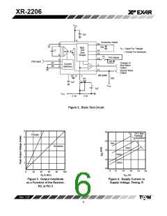
XR-2206
V
CC
2
1
ƪ ƫ
f +
1mF
C R1 ) R2
4
1
5
R1
16
Duty Cycle =
R1 ) R2
Mult.
And
Sine
C
15
14
VCO
6
Shaper
9
7
8
13
R
R
1
2
Current
Switches
2
Sawtooth Output
Pulse Output
+1
11
10 12
3
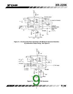
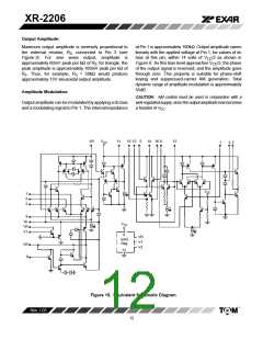
XR-2206
R
3
5.1K
V
24K
+
1mF
+
CC
10mF
V
CC
5.1K
5.1K
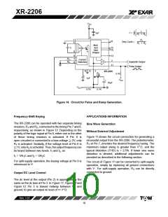
Figure 14. Circuit for Pulse and Ramp Generation.
APPLICATIONS INFORMATION
Frequency-Shift Keying
The XR-2206 can be operated with two separate timing
resistors, R and R , connected to the timing Pin 7 and 8,
Sine Wave Generation
1
2
respectively, as shown in Figure 13. Depending on the
polarity of the logic signal at Pin 9, either one or the other
of these timing resistors is activated. If Pin 9 is
open-circuited or connected to a bias voltage ꢀ 2V, only
Without External Adjustment
Figure 11 shows the circuit connection for generating a
sinusoidal output from the XR-2206. The potentiometer,
R at Pin 7, provides the desired frequency tuning. The
maximum output swing is greater than V /2, and the
R is activated. Similarly, if the voltage level at Pin 9 is
1
1
+
ꢁ1V, only R is activated. Thus, the output frequency can
2
typical distortion (THD) is < 2.5%. If lower sine wave
distortion is desired, additional adjustments can be
provided as described in the following section.
be keyed between two levels. f and f , as:
1
2
f = 1/R C and f = 1/R C
1
1
2
2
For split-supply operation, the keying voltage at Pin 9 is
referenced to V .
The circuit of Figure 11 can be converted to split-supply
-
operation, simply by replacing all ground connections
-
with V . For split-supply operation, R can be directly
3
connected to ground.
Output DC Level Control
The dc level at the output (Pin 2) is approximately the
same as the dc bias at Pin 3. In Figure 11, Figure 12 and
Figure 13, Pin 3 is biased midway between V+ and
+
ground, to give an output dc level of ꢂ V /2.
Rev. 1.03
10

 EXAR [ EXAR CORPORATION ]