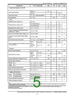
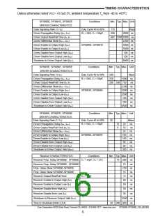
ELECTRICAL CHARACTERISTICS
PARAMETER
TEST CONDITIONS
MIN
TYP
MAꢀ
UNIT
Digital Input Signals: DI, DE, RE
High, Vih
2.0
Logic input thresholds
V
Low, Vil
0.8
±1
Logic Input Current
Input Hysteresis
Ta = 25°C, after first transition
Ta = 25°C
μA
100
mV
Driver
Differential Driver Output (Vo d )
No Load
Vc c
Vc c
Vc c
Vc c
V
V
Rl=100Ω (RS-422)
Rl=54Ω (RS-485)
Vc m = -7 to +12V
2
Differential Driver Output, Test 1
Differential Driver Output, Test 2
1.5
1.5
2.7
Change in Magnitude of Differential Output
Voltage (ΔVo d ) (Note 1)
Rl=54 or 100Ω
Rl=54 or 100Ω
±0.2
V
V
Driver Common Mode Output Voltage (Vcc)
1
3
Change in Common Mode Output Voltage
(ΔVo c )
Rl=54 or 100Ω
±0.2
V
Driver Short Circuit Current Limit
-7V ≤ Vo u t ≤ +12V (Note 5)
±250
mA
DE=0,
Vo u t =12V
125
Output Leakage Current (Full-duplex versions,
Y & Z pins) Note 2
RE=0,
Vc c =0 or
5.5V
μA
Vo u t = -7V
-100
96
Receiver
Receiver Input Resistance
-7V ≤ Vc m ≤ 12V
KΩ
μA
DE=0,
RE=0,
Vcc=0 or
5.5V
Vin= 12V
Vin= -7V
125
Input Current (A, B pins)
-100
-200
Receiver Differential Threshold (VA-VB)
Receiver Input Hysteresis
-7V ≤ Vc m ≤ 12V
-125
-40
mV
mV
25
Receiver
Output
Voltage
Vo h
Vo l
Io u t = -8mA, Vid = -40mV
Vcc-1.5
V
Io u t = 8mA, Vid = -200mV
Vc c =5.5V, 0 ≤ Vo u t ≤ Vc c
0.4
± 1
High-Z Receiver Output Current
Receiver Output Short Circuit Current
Supply and Protection
μA
0V ≤ Vr o ≤ Vc c
± 95
mA
IQ, Active Mode
Supply
No load, DI=0 or Vc c
DE=0, RE=Vcc, DI=Vc c
Junction temperature
400
900
1
μA
μA
Current
Shutdown Mode
Thermal Shutdown Temperature
Thermal Shutdown Hysteresis
165
oC
15
Notes:
1. Change in Magnitude of Differential Output Voltage and Change in Magnitude of Common Mode Output Voltage are the changes in output voltage when DI input changes state.
2. Except devices which don’t have DE or RE inputs.
3. The transceivers are put into shutdown by bringing RE high and DE low. If the inputs are in this state for less than 50ns the device does not enter shutdown. If the enable inputs
are held in this state for at least 600ns the device is assured to be in shutdown. In this low power mode most circuitry is disabled and supply current is typically 1nA.
4.Characterized, not 100% tested.
5. See Driver Short Circuit Limit Test Circuit.
Exar Corporation 48720 Kato Road, Fremont CA, 94538 • 510-668-7017 • www.exar.com
SP3080E-SP3088E_100_062309
5

 EXAR [ EXAR CORPORATION ]