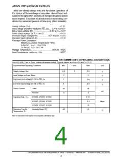
ABSOLUTE MAꢀIMUM RATINGS
These are stress ratings only and functional operation of
the device at these ratings or any other above those indi-
cated in the operation sections of the specifications below
is not implied. Exposure to absolute maximum rating con-
ditions for extended periods of time may affect reliability.
Supply Voltage (VCC).......................................................+ 7.0V
Input voltage at control input pins (RE, DE)... -0.3VtoVc c +0.3V
Driver input voltage (DI) ..............................-0.3V to Vc c +0.3V
Driver output voltage (A, B, Y, and Z) ............................+/-13V
Receiver output voltage (RO) ..................-0.3V to (Vcc + 0.3V)
Receiver input voltage (A, B) .........................................+/-13V
Package Power Dissipation:
Maximum Junction Temperature 150°C
8-Pin SO Θj a = 128.4°C/W
14-Pin SO Θj a = 86°C/W
Storage Temperature.......................................-65°C to +150°C
Lead Temperature (soldering, 10s)............................... +300°C
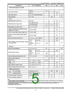
RECOMMENDED OPERATING CONDITIONS
Vcc=5V ±5%, Tm in to Tm a x , unless otherwise noted, Typical values are Vcc=5V and Ta=25°C
Recommended Operating Conditions
Min.
Nom.
Max.
Unit
Supply Voltage, Vc c
4.5
-7
2
5
5.5
V
V
V
Input Voltage on A and B pins
High-level input voltage (DI, DE or RE), Vih
12
Vc c
Low-level input voltage (DI, DE or RE), Vih
0
0.8
V
Output Current
Driver
-60
-8
60
8
mA
Receiver
Signaling Rate, 1/tu i
SP3080, SP3081, SP3082
0.115
SP3083, SP3084, SP3085
SP3086, SP3087, SP3088
Industrial Grade (E)
0.5
20
85
Mbps
°C
Operating Free Air
-40
Temperature, T
a
Note: The least positive (most negative) limit is designated as the maxium value.
Exar Corporation 48720 Kato Road, Fremont CA, 94538 • 510-668-7017 • www.exar.com
SP3080E-SP3088E_100_062309
4

 EXAR [ EXAR CORPORATION ]