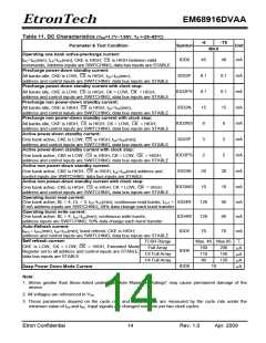
EM68916DVAA
EtronTech
z Bank Activation / Row Address Command
The Bank Activation / Row Address command, also called the Active command, is issued by holding
CAS
and
High with
and
CS RAS
Low at the rising edge of the clock (CK). The DDR SDRAM has four
WE
independent banks, so two Bank Select Addresses (BA0, BA1) are required. The Active command must be
applied before any read or write operation is executed. The delay from the Active command to the first Read
or Write command must meet or exceed the minimum of
to
delay time (tRCD min). Once a bank
CAS
RAS
has been activated, it must be precharged before another Active command can be applied to the same bank.
The minimum time interval between interspersed Active commands (Bank 0 to Bank 3, for example) is the
bank to bank delay time (tRRD min).
z Burst Read Operation
Burst Read operation in a DDR SDRAM is initiated by asserting
and
Low while holding and
RAS
CS
RAS
High at the rising edge of the clock (CK) after tRCD from the Active command. The address inputs (A0~A8)
WE
determine the starting address for the Burst. The Mode Register sets the type of burst (Sequential or
Interleaved) and the burst length (2, 4, or 8). The first output data is available after the Latency from the
CAS
Read command, and the consecutive data bits are presented on the falling and rising edges of Data Strobe
(DQS) as supplied by the DDR SDRAM until the burst is completed.
z Burst Write Operation
The Burst Write command is issued by havingCS, CAS and WE Low while holding RAS High at the rising
edge of the clock (CK). The address inputs determine the starting column address. There is no write latency
relative to DQS required for the Burst Write cycle. The first data for a Burst Write cycle must be applied at the
first rising edge of the data strobe enabled after tDQSS from the rising edge of the clock when the Write
command was issued. The remaining data inputs must be supplied on each subsequent falling and rising
edge of Data Strobe until the burst length is completed. After the burst has finished, any additional data
supplied to the DQ pins will be ignored.
z Burst Interruption
Read Interrupted by Read
Burst Read can be interrupted before completion of the burst by a new Read command to any bank. When
the previous burst is interrupted, data bits from the remaining addresses are overridden by data from the new
addresses with the full burst length. The data from the previous Read command continues to appear on the
outputs until the CAS latency from the interrupting Read command is satisfied. At this point the data from the
interrupting Read command appears. The Read to Read interval is a minimum of 1 clock.
Read Interrupted by Burst Stop & Write
To interrupt Burst Read with a write command, the Burst Stop command must be asserted to avoid data
contention on the I/O bus by placing the DQ (output drivers) in a high impedance state. To ensure the DQ are
tri-stated one cycle before the beginning of the write operation, the Burst Stop command must be applied at
least 2 clock cycles for CL = 2 and at least 3 clock cycles for CL = 3 before the Write command.
Read Interrupted by Precharge
Burst Read can be interrupted by a Precharge of the same bank. A minimum of 1 clock cycle is required for
the read precharge interval. A Precharge command to output disable latency is equivalent to the
latency.
CAS
Etron Confidential
10
Rev. 1.0
Apr. 2009

 ETRON [ ETRON TECHNOLOGY, INC. ]