Document No.: FT_000288
FT232H SINGLE CHANNEL HI-SPEED USB TO MULTIPURPOSE UART/FIFO IC
Datasheet Version 1.8
Clearance No.: FTDI #199
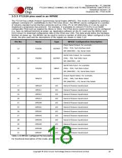
3.5.5 FT232H pins used in an MPSSE
The FT232H has a Multi-Protocol Synchronous Serial Engine (MPSSE). This mode is enabled by sending a
software command (FT_SetBitMode) to the FTDI D2xx driver. The MPSSE can be configured to a number
of industry standard serial interface protocols such as JTAG, I2C or SPI (MASTER), or it can be used to
implement a proprietary bus protocol. For example, it is possible to connect FT232H’s to an SRAM
configurable FPGA such as supplied by Altera or Xilinx. The FPGA device would normally not be configured
(i.e. have no defined function) at power-up. Application software on the PC could use the MPSSE (and
D2XX driver) to download configuration data to the FPGA over USB. This data would define the hardware
function on power up. The MPSSE can be used to control a number of GPIO pins. When configured in this
mode, the pins used and the descriptions of the signals are shown in Table 3.10
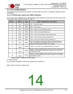
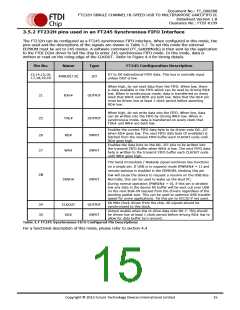
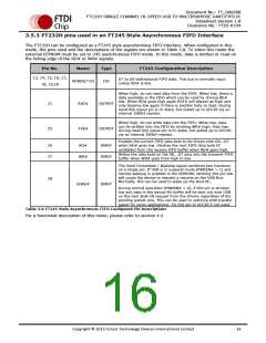
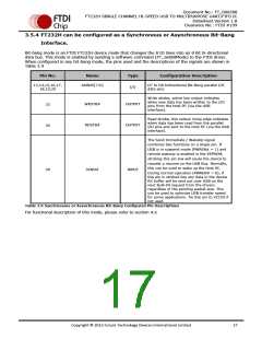
Pin No.
Name
Type
MPSSE Configuration Description
Clock Signal Output. For example:
JTAG – TCK, Test interface clock
SPI (MASTER) – SK, Serial Clock
13
TCK/SK
OUTPUT
Serial Data Output. For example:
JTAG – TDI, Test Data Input
SPI (MASTER) – DO
14
15
16
TDI/DO
TDO/DI
TMS/CS
OUTPUT
INPUT
Serial Data Input. For example:
JTAG – TDO, Test Data output
SPI (MASTER) – DI, Serial Data Input
Output Signal Select. For example:
JTAG – TMS, Test Mode Select
OUTPUT
SPI (MASTER) – CS, Serial Chip Select
17
18
19
20
21
25
26
27
28
29
30
31
GPIOL0
GPIOL1
GPIOL2
GPIOL3
GPIOH0
GPIOH1
GPIOH2
GPIOH3
GPIOH4
GPIOH5
GPIOH6
GPIOH7
I/O
I/O
I/O
I/O
I/O
I/O
I/O
I/O
I/O
I/O
I/O
I/O
General Purpose input/output
General Purpose input/output
General Purpose input/output
General Purpose input/output
General Purpose input/output
General Purpose input/output
General Purpose input/output
General Purpose input/output
General Purpose input/output
General Purpose input/output
General Purpose input/output
General Purpose input/output
Table 3.10 MPSSE Configured Pin Descriptions
For functional description of this mode, please refer to section 4.8
Copyright © 2012 Future Technology Devices International Limited
18

 ETC [ ETC ]