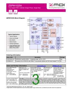
ZSPM1025A
True Digital PWM Controller (Single-Phase, Single-Rail)
Contents
List of Figures .......................................................................................................................................................... 5
List of Tables ........................................................................................................................................................... 7
1
2
3
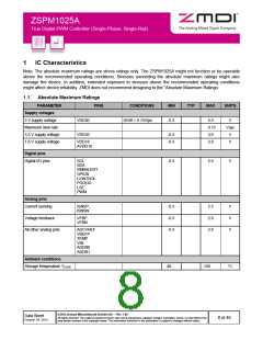
IC Characteristics ............................................................................................................................................. 8
1.1. Absolute Maximum Ratings....................................................................................................................... 8
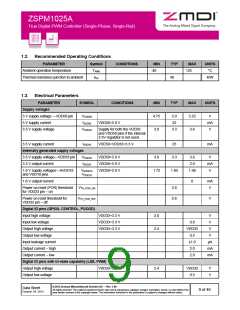
1.2. Recommended Operating Conditions ....................................................................................................... 9
1.3. Electrical Parameters ................................................................................................................................ 9
Product Summary...........................................................................................................................................12
2.1. Overview..................................................................................................................................................12
2.2. Pin Description.........................................................................................................................................14
2.3. Available Packages .................................................................................................................................15
Functional Description....................................................................................................................................16
3.1. Power Supply Circuitry, Reference Decoupling, and Grounding ............................................................16
3.2. Reset/Start-up Behavior ..........................................................................................................................16
3.3. Digital Power Control...............................................................................................................................16
3.3.1. Overview ...........................................................................................................................................16
3.3.2. Output Voltage Feedback .................................................................................................................16
3.3.3. Digital Compensator .........................................................................................................................17
3.3.4. Power Sequencing and the CONTROL Pin......................................................................................17
3.3.5. Pre-biased Start-up and Soft Stop....................................................................................................18
3.3.6. Current Sensing ................................................................................................................................19
3.3.7. Temperature Measurement ..............................................................................................................20
3.4. Fault Monitoring and Response Generation............................................................................................20
3.4.1. Output Over/Under-Voltage ..............................................................................................................21
3.4.2. Output Current Protection and Limiting ............................................................................................21
3.4.3. Over-Temperature Protection ...........................................................................................................21
3.5. Configuration ...........................................................................................................................................21
PMBus™ Functionality...................................................................................................................................22
4.1. Introduction..............................................................................................................................................22
4.2. Timing and Bus Specification ..................................................................................................................22
4.3. Address Selection via External Resistors................................................................................................23
4.4. Configuration Registers...........................................................................................................................24
4.5. Monitoring................................................................................................................................................26
4.6. Additional Registers.................................................................................................................................26
4.7. Detailed Description of the Supported PMBus™ Commands.................................................................27
4.7.1. OPERATION.....................................................................................................................................27
4.7.2. ON_OFF_CONFIG............................................................................................................................27
4.7.3. CLEAR_FAULTS ..............................................................................................................................27
4.7.4. VOUT_MODE ...................................................................................................................................28
4.7.5. VOUT_COMMAND ...........................................................................................................................28
4.7.6. STATUS_BYTE.................................................................................................................................28
4.7.7. STATUS_WORD...............................................................................................................................29
4
© 2013 Zentrum Mikroelektronik Dresden AG — Rev. 1.00
All rights reserved. The material contained herein may not be reproduced, adapted, merged, translated, stored, or used without the
prior written consent of the copyright owner. The information furnished in this publication is subject to changes without notice.
Data Sheet
October 24, 2013
4 of 46

 ETC [ ETC ]