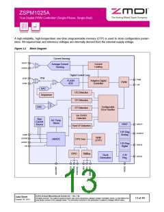
ZSPM1025A
True Digital PWM Controller (Single-Phase, Single-Rail)
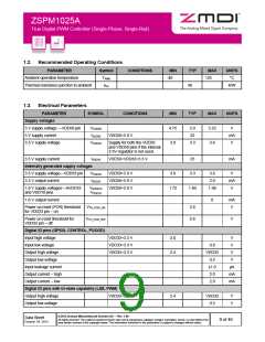
1.2. Recommended Operating Conditions
PARAMETER
Symbol
TAMB
CONDITIONS
MIN
-40
TYP
MAX
125
UNITS
°C
Ambient operation temperature
Thermal resistance junction to ambient
40
K/W
JA
1.3. Electrical Parameters
PARAMETER
Supply voltages
SYMBOL
CONDITIONS
MIN
4.75
3.0
TYP
MAX
5.25
3.6
UNITS
5 V supply voltage —VDD50 pin
5 V supply current
VVDD50
5.0
23
V
mA
V
IVDD50
VDD50=5.0 V
3.3 V supply voltage
VVDD33
Supply for both the VDD33
and VDD50 pins if the internal
3.3V regulator is not used.
3.3
3.3 V supply current
IVDD33
VDD50=VDD33=3.3 V
23
3.3
mA
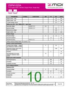
Internally generated supply voltages
3.3 V supply voltage—VDD33 pin
VVDD33
VDD50=5.0 V
VDD50=5.0 V
VDD50=5.0 V
3.0
3.6
2.0
V
mA
V
3.3 V output current
IVDD33
1.8 V supply voltages—AVDD18
and VDD18 pins
VAVDD18
VVDD18
1.72
1.80
1.98
1.8 V output current
0
mA
V
Power on reset (POR) threshold
for VDD33 pin – on
VTH_POR_ON
VTH_POR_OFF
2.8
2.6
Power on reset threshold for
V
VDD33 pin – off
Digital IO pins (GPIO0, CONTROL, PGOOD)
Input high voltage
VDD33=3.3 V
VDD33=3.3 V
VDD33=3.3 V
2.0
2.4
V
V
Input low voltage
0.8
VDD33
0.5
Output high voltage
V
Output low voltage
V
Input leakage current
Output current – high
Output current – low
±1.0
2.0
µA
mA
mA
2.0
Digital IO pins with tri-state capability (LSE, PWM)
Output high voltage
Output low voltage
VDD33=3.3 V
2.4
VDD33
0.5
V
V
© 2013 Zentrum Mikroelektronik Dresden AG — Rev. 1.00
All rights reserved. The material contained herein may not be reproduced, adapted, merged, translated, stored, or used without the
prior written consent of the copyright owner. The information furnished in this publication is subject to changes without notice.
Data Sheet
October 24, 2013
9 of 46

 ETC [ ETC ]