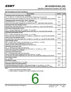
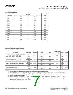
ESMT
M13S2561616A (2S)
Operation Temperature Condition -40°C~85°C
AC Timing Parameter & Specifications – continued
-5
-6
Parameter
Symbol
Unit
Note
min
max
min
max
Active to Precharge command
tRAS
tRC
40
70K
42
70K
ns
ns
Active to Active / Auto Refresh
command period
55
70
60
72
Auto Refresh to Active / Auto Refresh
command period
tRFC
ns
Active to Read, Write delay
Precharge command period
tRCD
tRP
15
15
18
18
ns
ns
Active to Read with Auto Precharge
command
tRAP
tRRD
15
10
18
12
ns
ns
Active bank A to Active bank B
command
Write recovery time
tWR
tWTR
15
2
15
2
ns
tCK
us
tCK
tCK
tCK
tCK
ns
Write data in to Read command delay
Average periodic refresh interval
Write preamble
tREFI
7.8
7.8
14
12
tWPRE
tWPST
tRPRE
tRPST
tWPRES
tMRD
0.25
0.4
0.9
0.4
0
0.25
0.4
0.9
0.4
0
Write postamble
0.6
1.1
0.6
0.6
1.1
0.6
Read preamble
Read postamble
Clock to DQS write preamble setup time
Mode Register Set command cycle time
Exit self refresh to Read command
Exit self refresh to non-Read command
13
23
2
2
tCK
tCK
ns
tXSRD
tXSNR
200
75
200
75
(tWR/tCK
)
(tWR/tCK
)
Auto Precharge write
recovery+precharge time
tDAL
+
+
tCK
(tRP/tCK
)
(tRP/tCK)
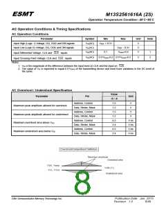
Notes:
1. All voltages referenced to VSS
.
2. Tests for AC timing, IDD, and electrical, AC and DC characteristics, may be conducted at nominal reference/supply
voltage levels, but the related specifications and device operation are guaranteed for the full voltage range specified.
3. The below figure represents the timing reference load used in defining the relevant timing parameters of the part. It is
not intended to be either a precise representation of the typical system environment nor a depiction of the actual load
presented by a production tester. System designers will use IBIS or other simulation tools to correlate the timing
reference load to a system environment. Manufacturers will correlate to their production test conditions (generally a
coaxial transmission line terminated at the tester electronics).
Elite Semiconductor Memory Technology Inc.
Publication Date : Jan. 2015
Revision : 1.0 10/49

 ESMT [ ELITE SEMICONDUCTOR MEMORY TECHNOLOGY INC. ]