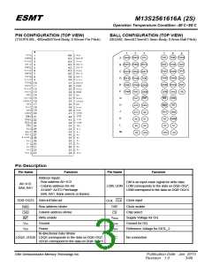
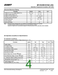
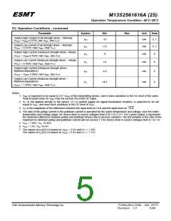
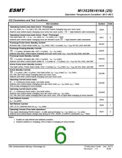
ESMT
M13S2561616A (2S)
Operation Temperature Condition -40°C~85°C
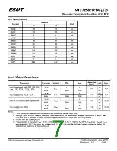
IDD Specifications
Version
Symbol
Unit
-5
80
-6
70
IDD0
mA
mA
mA
mA
mA
mA
mA
mA
mA
mA
mA
mA
IDD1
110
4
100
4
IDD2P
IDD2F
IDD2Q
IDD3P
IDD3N
IDD4R
IDD4W
IDD5
30
30
30
30
25
20
55
50
130
130
140
3
120
120
130
3
IDD6
IDD7
220
210
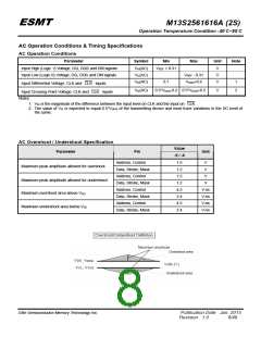
Input / Output Capacitance
Delta Cap
(max)
Parameter
Package Symbol
Min
Max
Unit
Note
Input capacitance (A0~A12, BA0~BA1,
CKE, CS , RAS , CAS , WE )
TSOP
CIN1
2
TBD
2
5
TBD
4
pF
pF
pF
pF
pF
pF
pF
pF
0.5
1,4
BGA
TSOP
CIN2
BGA
0.25
0.5
1,4
Input capacitance (CLK, CLK )
TBD
1
TBD
4
TSOP
COUT
BGA
Data & DQS input/output capacitance
1,2,3,4
1,2,3,4
TBD
1
TBD
4
TSOP
CIN3
BGA
Input capacitance (DM)
Notes:
0.5
TBD
TBD
1. These values are guaranteed by design and are tested on a sample basis only.
2. Although DM is an input -only pin, the input capacitance of this pin must model the input capacitance of the DQ and
DQS pins. This is required to match signal propagation times of DQ, DQS, and DM in the system.
3. Unused pins are tied to ground.
4. This parameter is sampled. VDDQ = 2.5V ± 0.2V, VDD = 2.5V ± 0.2V. f=100MHz, TA =25°C, VOUT(DC) = VDDQ/2, VOUT
(peak to peak) = 0.2V. DM inputs are grouped with I/O pins - reflecting the fact that they are matched in loading (to
facilitate trace matching at the board level).
Elite Semiconductor Memory Technology Inc.
Publication Date : Jan. 2015
Revision : 1.0 7/49

 ESMT [ ELITE SEMICONDUCTOR MEMORY TECHNOLOGY INC. ]