EN29LV160A
To access the autoselect codes in-system; the host system can issue the autoselect command via
the command register, as shown in the Command Definitions table. This method does not require VID.
See “Command Definitions” for details on using the autoselect mode.
Write Mode
Programming is a four-bus-cycle operation. The program command sequence is initiated by writing
two unlock write cycles, followed by the program set-up command. The program address and data
are written next, which in turn initiate the Embedded Program algorithm. The system is not required
to provide further controls or timings. The device automatically provides internally generated program
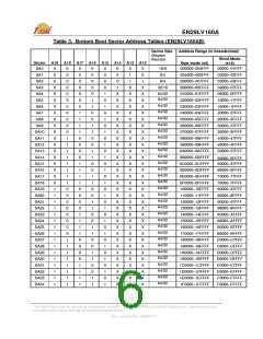
pulses and verifies the programmed cell margin. The Command Definitions in Table 5 show the
address and data requirements for the byte program command sequence.
When the Embedded Program algorithm is complete, the device then returns to reading array data
and addresses are no longer latched. The system can determine the status of the program operation
by using DQ7 or DQ6. See “Write Operation Status” for information on these status bits.
Any commands written to the device during the Embedded Program Algorithm are ignored.
Programming is allowed in any sequence and across sector boundaries. A bit cannot be
programmed from a “0” back to a “1”. Attempting to do so may halt the operation and set DQ5 to
“1”, or cause the Data# Polling algorithm to indicate the operation was successful. However, a
succeeding read will show that the data is still “0”. Only erase operations can convert a “0” to a “1”.
Sector Protection/Unprotection
The hardware sector protection feature disables both program and erase operations in any sector.
The hardware sector unprotection feature re-enables both program and erase operations in
previously protected sectors.
There are two methods to enabling this hardware protection circuitry. The first one requires only that
the RESET# pin be at V and then standard microprocessor timings can be used to enable or
ID
disable this feature. See Flowchart 7a and 7b for the algorithm and Figure 12 for the timings.
When doing Sector Unprotect, all the other sectors should be protected first.
The second method is meant for programming equipment. This method requires V be applied to
ID
both OE# and A9 pin and non-standard microprocessor timings are used. This method is described
in a separate document called EN29LV160A Supplement, which can be obtained by contacting a
representative of Eon Silicon Solution, Inc.
Temporary Sector Unprotect
Start
This feature allows temporary unprotection of previously protected
sector groups to change data while in-system. The Sector
Unprotect mode is activated by setting the RESET# pin to VID.
During this mode, formerly protected sectors can be programmed
or erased by simply selecting the sector addresses. Once is
removed from the RESET# pin, all the previously protected sectors
Reset#=VID (note 1)
Perform Erase or Program
Operations
are protected again.
diagrams for more details.
See accompanying figure and timing
Reset#=VIH
Notes:
Temporary Sector
Unprotect Completed (note 2)
1. All protected sectors unprotected.
2. Previously protected sectors protected
again.
This Data Sheet may be revised by subsequent versions
or modifications due to changes in technical specifications.
©2004 Eon Silicon Solution, Inc., www.essi.com.tw
10
Rev. I, Issue Date: 2008/07/17

 ESMT [ ELITE SEMICONDUCTOR MEMORY TECHNOLOGY INC. ]