Epson Research and Development
Page 89
Vancouver Design Center
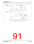
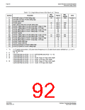
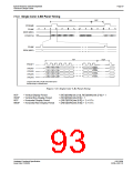
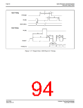
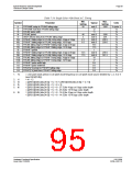
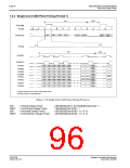
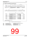
Table 7-24: Single Color 4-Bit Panel A.C. Timing
Min.
Setting
Max.
Setting
1268
Symbol
Parameter
Typical
Units
t1
t2
t3
FPFRAME setup to FPLINE falling edge
FPFRAME hold from FPLINE falling edge
FPLINE pulse width
28
note 2
12
11
Ts (note 1)
Ts
Ts
t4
t5
FPLINE period
40
3
4.5
6.5
note 3
note 4
note 5
note 5
19.5
17.5
1
1280
259
228.5
230.5
Ts
Ts
Ts
Ts
Ts
Ts
Ts
DRDY (MOD) delay from FPLINE falling edge
FPSHIFT falling edge to FPLINE rising edge, 4 bpp or 8 bpp
FPSHIFT falling edge to FPLINE rising edge, 15/16 bpp
FPLINE falling edge to FPSHIFT falling edge, 4 bpp or 8 bpp
FPLINE falling edge to FPSHIFT falling edge, 15/16 bpp
FPSHIFT period
t6a
t6b
t7a
t7b
t8
t9a
t9b
t10a
t10b
t11
t12
t13
t14
FPSHIFT falling edge to FPLINE falling edge, 4 bpp or 8 bpp
FPSHIFT falling edge to FPLINE falling edge, 15/16 bpp
FPLINE falling edge to FPSHIFT rising edge, 4 bpp or 8 bpp
FPLINE falling edge to FPSHIFT rising edge, 15/16 bpp
FPSHIFT pulse width high
FPSHIFT pulse width low
FPDAT[7:4] setup to FPSHIFT falling edge
FPDAT[7:4] hold from FPSHIFT falling edge
15.5
17.5
note 6
note 6
19
17
0.5
0.5
0.5
0.5
239.5
241.5
Ts
Ts
Ts
Ts
Ts
Ts
Ts
Ts
1. Ts
= LCD pixel clock period. LCD pixel clock frequency is LCD pixel clock source divided by 1, 2, 3 or 4
(see REG[014h]).
2. t1
3. t4
4. t5
5. t6
= t4 - 12
= [((REG[032h] bits [6:0]) + 1) × 8 + ((REG[034h] bits [4:0]) + 1) × 8]
= [((REG[034h] bits [4:0]) + 1) × 8 + 3]
= [((REG[034h] bits [4:0]) + 1) × 8 - 27.5] for 4 bpp or 8 bpp color depth
= [((REG[034h] bits [4:0]) + 1) × 8 - 25.5] for 15/16 bpp color depth
= [((REG[034h] bits [4:0]) + 1) × 8 - 16.5] for 4 bpp or 8 bpp color depth
= [((REG[034h] bits [4:0]) + 1) × 8 - 14.5] for 15/16 bpp color depth
6. t9
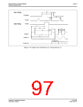
Hardware Functional Specification
Issue Date: 01/02/06
S1D13506
X25B-A-001-10

 EPSON [ EPSON COMPANY ]