Page 12
Epson Research and Development
Vancouver Design Center
The host interface control signals of the S1D13506 are asynchronous with respect to the
S1D13506 bus clock. This gives the system designer full flexibility to choose the
appropriate source (or sources) for CLKI and BUSCLK. The choice of whether both clocks
should be the same, whether to use DCLKOUT as clock source, and whether an external or
internal clock divider is needed, should be based on the desired:
• pixel and frame rates.
• power budget.
• part count.
• maximum S1D13506 clock frequencies.
The S1D13506 also has internal CLKI dividers providing additional flexibility.
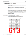
4.2 S1D13506 Configuration
The S1D13506 latches MD15 through MD0 to allow selection of the bus mode and other
configuration data on the rising edge of RESET#. For details on configuration, refer to the
S1D13506 Hardware Functional Specification, document number X25B-A-001-xx.
The table below shows those configuration settings relevant to the Philips
PR31500/PR31700 Host Bus Interface.
Table 4-1: S1D13506 Configuration for Direct Connection
Value on this pin at rising edge of RESET# is used to configure:
S1D13506
Pin Name
1 (VDD
)
0 (VSS)
MD[3:1]
MD4
111 = Philips PR31500/PR31700 Host Bus Interface when MD11 = 1
Little Endian
Big Endian
MD5
WAIT# is active high (1 = insert wait state)
WAIT# is active low (0 = insert wait state)
MD11
MD12
Alternate Host Bus Interface selected
Primary Host Bus Interface selected
BUSCLK input divided by two: use with DCLKOUT BUSCLK input not divided: use with external oscillator
MD15
WAIT# is floating if S1D13506 is not selected
= configuration for Philips PR31500/PR31700 Host Bus Interface
WAIT# is always driven
S1D13506
X25B-G-009-02
Interfacing to the Philips MIPS PR31500/PR31700 Processor
Issue Date: 01/02/08

 EPSON [ EPSON COMPANY ]