Page 224
Epson Research and Development
Vancouver Design Center
20 Clocks
20.1 Clock Selection
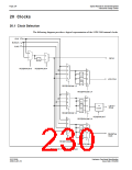
The following diagram provides a logical representation of the S1D13506 internal clocks.
CLKI
BUSCLK
CLKI2
0
1
0
MCLK
÷2
1
00
01
10
11
REG[010h] bit 0
REG[014h] bit 4
00
01
÷2
÷3
÷4
10
11
LCD PCLK
REG[014h] bits 1,0
REG[014h] bits 5,4
00
00
01
10
11
01
÷2
x2
10
11
÷3
÷4
CRT/TV
PCLK
Enable
REG[018h] bits 1,0
REG[018h] bit 7
REG[018h] bits 5,4
00
00
01
01
10
11
÷2
10
11
÷3
÷4
MediaPlug
Clock
REG[01Ch] bits 1,0
REG[01Ch] bits 5,4
Figure 20-1: Clock Selection
S1D13506
X25B-A-001-10
Hardware Functional Specification
Issue Date: 01/02/06

 EPSON [ EPSON COMPANY ]