Preliminary EN29GL064
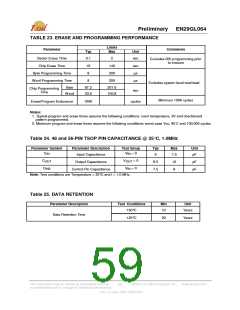
TABLE 23. ERASE AND PROGRAMMING PERFORMANCE
Limits
Max
Parameter
Comments
Typ
Unit
Sector Erase Time
Chip Erase Time
0.1
2
sec
Excludes 00h programming prior
to erasure
16
8
140
200
200
sec
µs
Byte Programming Time
Word Programming Time
8
µs
Excludes system level overhead
Minimum 100K cycles
Byte
67.2
33.6
201.6
100.8
Chip Programming
sec
Time
Word
Erase/Program Endurance
100K
cycles
Notes:
1. Typical program and erase times assume the following conditions: room temperature, 3V and checkboard
pattern programmed.
2. Maximum program and erase times assume the following conditions: worst case Vcc, 90 C and 100,000 cycles.
Table 24. 48 and 56-PIN TSOP PIN CAPACITANCE @ 25°C, 1.0MHz
Parameter Symbol
Parameter Description
Test Setup
= 0
Typ
Max
Unit
C
V
IN
IN
Input Capacitance
6
7.5
pF
C
V
= 0
OUT
OUT
Output Capacitance
8.5
7.5
12
9
pF
pF
C
V
= 0
IN2
IN
Control Pin Capacitance
Note: Test conditions are Temperature = 25°C and f = 1.0 MHz.
Table 25. DATA RETENTION
Parameter Description
Test Conditions
Min
Unit
150°C
10
Years
Years
Data Retention Time
125°C
20
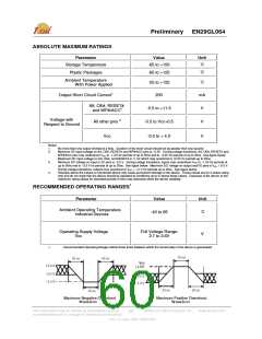
This Data Sheet may be revised by subsequent versions
or modifications due to changes in technical specifications.
©2004 Eon Silicon Solution, Inc., www.eonssi.com
59
Rev. A, Issue Date: 2009/3/20

 EON [ EON SILICON SOLUTION INC. ]