EN5339QI
Design Considerations for Lead-Frame Based Modules
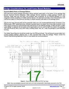
Exposed Metal Pads on Package Bottom
QFN lead-frame based package technology utilizes exposed metal pads on the bottom of the package that
provide improved thermal dissipation, lower package thermal resistance, smaller package footprint and
thickness, larger lead size and pitch, and excellent lead co-planarity. As the EN5339 package is a fully
integrated module consisting of multiple internal devices, the lead-frame provides circuit interconnection and
mechanical support of these devices resulting in multiple exposed metal pads on the package bottom.
Only the two large thermal pads and the perimeter leads are to be mechanically/electrically connected to the
PCB through a SMT soldering process. All other exposed metal is to remain free of any interconnection to the
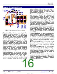
PCB. Figure 9 shows the recommended PCB metal layout for the EN5339 package. A GND pad with a solder
mask "bridge" to separate into two pads and 24 signal pads are to be used to match the metal on the package.
The PCB should be clear of any other metal, including traces, vias, etc., under the package to avoid electrical
shorting.
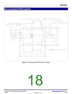
The Solder Stencil Aperture should be smaller than the PCB ground pad. This will prevent excess solder from
causing bridging between adjacent pins or other exposed metal under the package. Please consult the
Enpirion Manufacturing Application Note for more details and recommendations.
Figure 9. Recommended Footprint for PCB (Top View)
Note: Grey area highlights exposed metal that is not to be mechanically or electrically connected to the PCB.
Enpirion 2012 all rights reserved, E&OE
www.enpirion.com, Page 17
06903
September 12, 2012
Rev: B

 ENPIRION [ ENPIRION, INC. ]