EN5339QI
Layout Recommendations
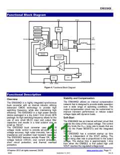
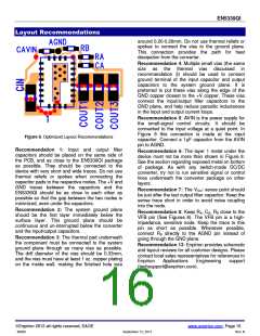
around 0.20-0.26mm. Do not use thermal reliefs or
spokes to connect the vias to the ground plane.
This connection provides the path for heat
dissipation from the converter.
Recommendation 4: Multiple small vias (the same
size as the thermal vias discussed in
recommendation 3) should be used to connect
ground terminal of the input capacitor and output
capacitors to the system ground plane. It is
preferred to put these vias along the edge of the
GND copper closest to the +V copper. These vias
connect the input/output filter capacitors to the
GND plane, and help reduce parasitic inductances
in the input and output current loops.
Recommendation 5: AVIN is the power supply for
the small-signal control circuits. It should be
connected to the input voltage at a quiet point. In
Figure 8 this connection is made at the input
capacitor. Connect a 1µF capacitor from the AVIN
pin to AGND.
Figure 8. Optimized Layout Recommendations
Recommendation 1: Input and output filter
capacitors should be placed on the same side of
the PCB, and as close to the EN5339QI package
as possible. They should be connected to the
device with very short and wide traces. Do not use
thermal reliefs or spokes when connecting the
capacitor pads to the respective nodes. The +V and
GND traces between the capacitors and the
EN5339QI should be as close to each other as
possible so that the gap between the two nodes is
minimized, even under the capacitors.
Recommendation 6: The layer 1 metal under the
device must not be more than shown in Figure 8.
See the section regarding exposed metal on bottom
of package. As with any switch-mode DC/DC
converter, try not to run sensitive signal or control
lines underneath the converter package on other
layers.
Recommendation 7: The VOUT sense point should
be just after the last output filter capacitor. Keep the
sense trace short in order to avoid noise coupling
into the node.
Recommendation 2: The system ground plane
should be the first layer immediately below the
surface layer. This ground plane should be
continuous and un-interrupted below the converter
and the input/output capacitors.
Recommendation 8: Keep RA, CA, RB close to the
VFB pin (See Figures 6). The VFB pin is a high-
impedance, sensitive node. Keep the trace to this
pin as short as possible. Whenever possible,
connect RB directly to the AGND pin instead of
going through the GND plane.
Recommendation 3: The thermal pad underneath
the component must be connected to the system
ground plane through as many vias as possible.
The drill diameter of the vias should be 0.33mm,
and the vias must have at least 1 oz. copper plating
on the inside wall, making the finished hole size
Recommendation 13: Enpirion provides schematic
and layout reviews for all customer designs. Please
contact local sales representatives for references to
Enpirion
(techsupport@enpirion.com).
Applications
Engineering
support
Enpirion 2012 all rights reserved, E&OE
www.enpirion.com, Page 16
06903
September 12, 2012
Rev: B

 ENPIRION [ ENPIRION, INC. ]