EM6603
SPECIFICATION change
date
Chapter
old text
new text
Version
(page)
9/11/99 ver.2.2 All
27/6/97 B/151 All
27/6/97 B/151 All
27/6/97 B/151 (1,2)
New specifications (paper format only)
B/151 new version in Doc Control
Version 2.2
New pagination & new table nb.
typical 2.7µA active mode
typical 0.3µA standby mode
typical 1.8µA active mode
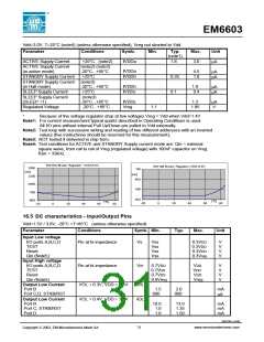
16.4(30,31)
typical 0.35µA standby mode
For Vdd less then 1.4V it is recommended
that Vdd is connected directly to Vreg
For Vdd>1.8V then the configuration
shown in Fig.3 should be used.
Table 10 option register – Option
new table and text describing option
register
27/6/97 B/151 (4)
2 (5)
27/6/97 B/151 6 (9)
27/6/97 B/151 6.4 (11)
27/6/97 B/151 6.6 (13)
27/6/97 B/151 8 (16)
below Figure 7. PortB new explanation of
mask options
below Figure 8. PortC new explanation of
mask options
First paragraph changed due to new
counter feature added – PA3 clk source
(debounced or not, Rising/Falling)
PA3 input terminal (see tables 28 and 29)
added in Table 24. Timer clock selection
Table 28 PA3 counter input selection –
PA3cnt
27/6/97 B/151 8 (16)
27/6/97 B/151 8.1 (17)
PA3 input terminal
Table 29 PA3 counter input selection
new tables describing PA3cnt register
Figure 10 Timer/Event Counter adapted
new description below Figure 11 Interrupt
Request generation
new formulation and more precise
explanation of SVLD (no functional
change)
27/6/97 B/151 9.1 (19)
27/6/97 B/151 10 (20)
27/6/97 B/151 11 (22)
27/6/97 B/151 11.1 (23)
27/6/97 B/151 11.2 (25)
27/6/97 B/151 14 (27)
Figure 12. Serail write buffer
1024 Hz input added in MUX
New explanation of SWB concerning
length and IRQ
New explanation of SWB in interactive
mode
New explanation of Metal mask options
below Table 40 Input/output Ports
Removed (software controlled)
New register PA3cnt at address 65 hex
VDD_range 1 / +1.4 ..+3.6V
27/6/97 B/151 14 (27)
27/6/97 B/151 15 (28)
27/6/97 B/151 16.2 (30)
Table 39 Watchdog metal option
VDD
VDD
VDD_range 2 (Vreg=VDD) / +1.2 ..+1.8V
VDD_range 1 / +1.4 ..+3.6V
27/6/97 B/151 16.2 (30)
27/6/97 B/151 16.5 (31)
27/6/97 B/151 16.5 (32)
27/6/97 B/151 16.6 (32)
27/6/97 B/151 16.7 (33)
VDD_range 2 (Vreg=VDD) / +1.2 ..+1.8V
New way of specifying
VOL = f(IOL ,Vdd),
VOH = f(IOH ,Vdd),
IOL = f(VOL ,Vdd), IOH = f(VOH ,Vdd),
New way of specifying Resistors
[kΩ] instead with currents
Input Pull-Up/Down resistor
expressed by currents
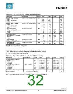
Absolute SVLD levels
2.50V, 2.00V, 1.25V
Max CQin 8.5 pf
Max CQout 15.9 pf
New relative way of specifying SVLD
precision and range for 3 levels x%
Max CQin 10.0 pf
Max CQout 20.0 pf
03/02 REV. G/439
37
www.emmicroelectronic.com
Copyright 2002, EM Microelectronic-Marin SA

 EMMICRO [ EM MICROELECTRONIC - MARIN SA ]