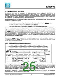
EM6603
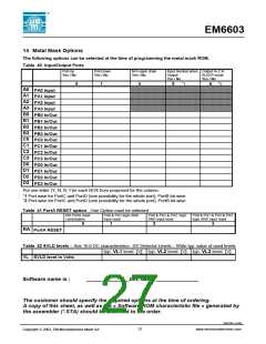
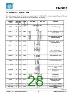
15 PERIPHERAL MEMORY MAP
The following table shows the peripheral memory map of the EM6603. The address space is between $00 and
$7F (Hex). Any addresses not shown can be considered to be reserved.
Register
name
add add power
write_bits
read_bits
Remarks
hex dec
up
value
b'3210
xxxx
Read/Write_bits
RAM
LTimLS
HTimLS
TimCtr
00- 0-95
5f
0: D0
1: D1
2: D2
3: D3
direct addressing
60
61
62
63
65
68
69
6A
6B
6C
6D
96
0000
0000
0000
0000
xxx0
0000
1111
0000
0000
0000
xx00
0: TL0
1: TL1
2: TL2
3: TL3
0: TL4
1: TL5
2: TL6
3: TL7
0: TS0
low nibble of 8bit timer load and
status register
1: TS1
2: TS2
3: TS3
0: TS4
1: TS5
2: TS6
3: TS7
97
high nibble of 8bit timer load
and status register
98
0:
1:
2:
TEC0
timer control register with
frequency selector
TEC1
TEC2
3: TimAuto
0: NoWD
1: debPAN
2: debPCN
3:IRQedgeR
0: PA3cntin
Option
99
option register
PA3cnt
ClkSWB
SWBuff
LowSWB
HighSWB
SVLD
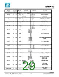
101
104
105
106
107
108
109
PA3 counter input
1:
2:
3:
Fout
Frequency output on STRB
-
-
0: CkSWB0
1: CkSWB1
Clock selector for SWB
SWB intermediate buffer
2:
3:
-
V03
0: Buff0
1: Buff1
2: Buff2
3: Buff3
0: size[0]
1: size[1]
2: size[2]
3: size[3]
0: size[4]
1: size[5]
2: StSWB
3:AutoSWB
low nibble to define the size of
data to be send in Automatic
mode
the size of the data to be sent &
SWB control
0: VLC0
1: VLC1
2: -
0: VLC0
voltage level
1: VLC1
2: busy
3: VLDR
detector control
3: -
CIRQD
0: INTEN
global interrupt enable
debouncer clock
1: DebCK
2:
3:
-
-
Index LOW
Index HIGH
6E
6F
110
111
xxxx
xxxx
internally used for INDEX
register
internally used for INDEX
register
03/02 REV. G/439
28
www.emmicroelectronic.com
Copyright 2002, EM Microelectronic-Marin SA

 EMMICRO [ EM MICROELECTRONIC - MARIN SA ]