EM78P809N
8-Bit Microcontroller
•
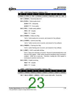
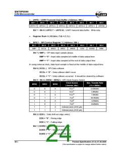
URTD − UART Transmit Data Buffer ( Address: 09h )
Bit 7
Bit 6
Bit 5
Bit 4
Bit 3
Bit 2
Bit 1
Bit 0
URTD 7 URTD 6
URTD 5
URTD 4
URTD 3
URTD 2
URTD 1
URTD0
Bit 7 ~ Bit 0 ( URTD 7 ~ URTD 0) : UART transmit data buffer. Write only.
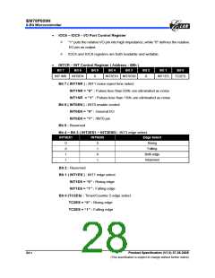
Register Bank 3 ( R3 bits ( 7,6) = (1,1) )
•
•
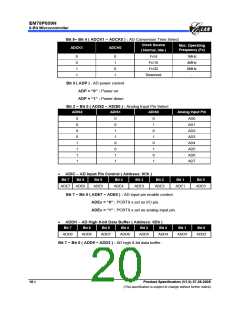
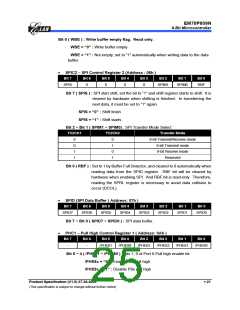
SPIC1 − SPI Control Register 1 ( Address: 05h )
Bit 7
Bit 6
Bit 5
Bit 4
Bit 3
Bit 2
Bit 1
Bit 0
SMP
DCOL
BRS2
BRS1
BRS0
EDS
DORD
WBE
Bit 7 ( SMP ) : SPI data input sample phase.
SMP = “0” : Input data sampled at middle of data output time
SMP = “1” : Input data sampled at the end of data output time
In using external clock, data input sample is fixed at the middle of data output time.
Bit 6 ( DCOL ) : SPI Data collision.
DCOL = “0” : Data collision didn’t occur
DCOL = “1” : Data collision occurred. It should be cleared by software.
Bit 5 ~ Bit 3 ( BRS0 ~ BRS2 ) : SPI Clock Source Select
Clock Source
( Normal, Idle )
Max. Transfer Rate
( Fc = 8MHz )
BRS2
BRS1
BRS0
0
0
0
0
1
1
1
1
0
0
1
1
0
0
1
1
0
1
0
1
0
1
0
1
Fc/213
Fc/211
Fc/210
Fc/28
Fc/26
0.95Kbit/s
3.8Kbit/s
7.6Kbit/s
30.5Kbit/s
122Kbit/s
244Kbit/s
-
Fc/25
External clock (/SCK pin)
External clock (/SCK pin)
-
Bit 2 ( EDS ) : Data shift out edge select.
EDS = “0” : Rising edge
EDS = “1” : Falling edge
Bit 1 ( DORD ) : Data transmission order.
DORD = “0” : Shift left (MSB first)
DORD = “1” : Shift right (LSB first)
20 •
Product Specification (V1.0) 07.26.2005
(This specification is subject to change without further notice)

 ELAN [ ELAN MICROELECTRONICS CORP ]