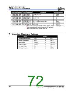
EM78P417N/418N/419N
8-Bit Microprocessor with OTP ROM
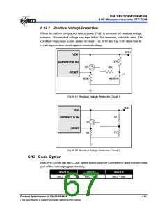
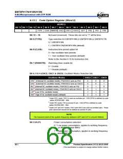
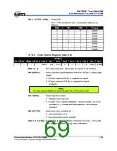
6.13.1 Code Option Register (Word 0)
WORD 0
Bit 12 Bit 11 Bit 10 Bit 9 Bit 8 Bit 7 Bit 6 Bit 5 Bit 4 Bit 3 Bit 2 Bit 1 Bit 0
–
–
–
TYPE CLKS ENWDTB OSC2 OSC1 OSC0
HLP
PR2
PR1
PR0
Bit 12 ~ 10:
Not used (reserved). These bits are set to “1” all the time
Bit 9 (TYPE):
Type selection for EM78P419N or EM78P418N or EM78P417N.
0 = EM78P419N
1 = EM78P417N/EM78P418N (default)
Bit 8 (CLKS):
Instruction time period option bit
0 = two oscillator time periods
1 = four oscillator time periods (default)
Refer to the Section 6.15 for Instruction Set
Bit 7 (ENWDTB): Watchdog timer enable bit
0 = Enable
1 = Disable (default)
Bit 6, 5 & 4 (OSC2, OSC1 & OSC0): Oscillator Modes Selection bits
Oscillator Modes
OSC2 OSC1 OSC0
ERC1 (External RC oscillator mode); P54/OSCO acts as P54
ERC1 (External RC oscillator mode); P54/OSCO acts as OSCO
IRC2 (Internal RC oscillator mode); P54/OSCO acts as P54
IRC2 (Internal RC oscillator mode); P54/OSCO acts as OSCO
LXT3 (Low XTAL oscillator mode)
0
0
0
0
1
1
0
0
1
1
1
1
0
1
0
1
0
1
HXT3 High XTAL oscillator mode) (default)
1 Under ERC mode, OSCI is used as oscillator pin. OSCO/P54 is defined by code
option WORD0 Bit6 ~ Bit4.
2 Under IRC mode, P55 is normal I/O pin. OSCO/P54 is defined by code
option WORD0 Bit6 ~ Bit4.
3 Under LXT and HXT modes; OSCI and OSCO are used as oscillator pins. These
pins cannot and should not be defined as normal I/O pins.
NOTE
The transient point of the system frequency between HXT and LXY is around 400kHz.
Bit 3 (HLP):
Power consumption selection
0 = Low power consumption, applies to working frequency
at 4MHz or below 4MHz
1 = High power consumption, applies to working frequency
above 4MHz
62 •
Product Specification (V1.0) 06.23.2005
(This specification is subject to change without further notice)

 ELAN [ ELAN MICROELECTRONICS CORP ]