EC49513A/L
300mA Linear Regulator with Enable
And Fast Discharge Function
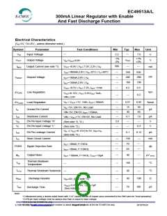
Electrical Characteristics
(VIN=5V, TA=25℃, unless otherwise noted.)
Symbol
Parameter
Input Voltage
Test Conditions
Min
Typ
Max
Unit
—
—
VIN
2.2
7.0
V
-1%
-2%
+1%
+2%
Output Voltage
V
VOUT
IMAX
VOUT
—
VIN=VOUT+0.8V
VOUT +0.8V VIN
IOUT=300mA,2.8V
IOUT=180mA,2.8V
OUT=150mA,2.8V
VOUT +0.5V VIN
VIN
300
—
≦
≦
7.0V, 2.2V
≦VIN
Output Current (see note *1)
mA
—
—
—
—
≦
VIN, 25°C≦TA≦80°C
550
240
160
650
280
180
mV
Dropout Voltage
Line Regulation
VDROP
≦
VIN
VIN
I
≦
≦
≦
7.0V, IOUT =1mA
0.2
—
0.3
0.2
%/V
∆VLINE
V
OUT+0.15V
≦
≦5.0V,IOUT 1mA,
—
—
VIN≧2.8V
VIN = VOUT +1V, 1mA
≦IOUT≦100mA
0.01
15
0.02
30
Load Regulation
%/mA
∆VLOAD
IQ
—
—
VIN =5V, EN=5V, No Load
Ground Pin Current
μA
30
60
VIN =5V, EN=5V, IOUT =150mA,
VIN = VOUT+1V, EN=0V, No Load
(See note *2, *4 )
Shutdown Current
—
0.1
—
1.0
—
μA
V
ISD
EN Pin Input Voltage “H”
EN Pin Input Voltage “L”
2.0
—
VI
H
VIL
IEN
ISC
—
0.3
V
(See note *2 )
VIN =( VOUT+0.15V) to 5V, VEN>VI
H
EN Pin Leakage Current
Short Circuit Current
—
0.1
0.15
μA
(See note *3 )
—
—
—
—
150
70
—
—
—
mA
IOUT =30mA, F=1KHz
PSRR
Ripple Rejection Rate
Output Noise
dB
65
IOUT =30mA, F=10KHz
—
—
—
—
40
150
20
—
—
μV (rms)
eN
IOUT =100mA, F=1KHz, COUT=10μA
Thermal Shutdown
Temperature
TSD
THYS
RDIS
°
°
C
C
—
—
Thermal Shutdown Hysteresis
Discharge Resistor
—
30
100
Ω
VEN=0V, (See note *3)
VOUT=3.3V to 0V, COUT=1μF
(See note *3)
—
70
100
μS
TDIS
Discharge Time
Note:
*1) Measured using a double sided board with 1”x2” square inches of copper area connected to the GND pins for “heat spreading”.
*2) EN pin input voltage must be always less than or equal to input voltage.
*3) It is for the EC49513L only.
*4) EN Pin with internal pull high resistor is about several hundreds of KΩ for EC49513A only.
E-CMOS Corp. (www.ecmos.com.tw) Page 6 of 24
2010/10/29

 E-CMOS [ E-CMOS Corporation ]