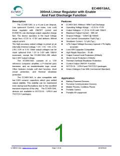
EC49513A/L
300mA Linear Regulator with Enable
And Fast Discharge Function
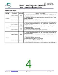
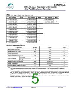
Table1
Mark code vs. Output Voltage code of Products part
Part Number
Mark
Part Number
Mark
Part Number
Mark
EC49513A/L-12B2G
EC49513A/L-12FG
EC49513A/L-12T2G
EC49513A/L-28B2G
EC49513A/L-28FG
EC49513A/L-28T2G
EC49513A/L-42B2G
EC49513A/L-42FG
EC49513A/L-42T2G
5
K
S
EC49513A/L-15B2G
EC49513A/L-15FG
EC49513A/L-15T2G
EC49513A/L-18B2G
EC49513A/L-18FG
EC49513A/L-18T2G
EC49513A/L-25B2G
EC49513A/L-25FG
EC49513A/L-25T2G
EC49513A/L-27B2G
EC49513A/L-27FG
EC49513A/L-27T2G
EC49513A/L-285B2G
EC49513A/L-285FG
EC49513A/L-285T2G
EC49513A/L-30B2G
EC49513A/L-30FG
EC49513A/L-30T2G
EC49513A/L-33B2G
EC49513A/L-33FG
EC49513A/L-33T2G
EC49513A/L-36B2G
EC49513A/L-36FG
EC49513A/L-36T2G
8
A
G
J
L
M
Q
V
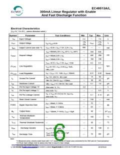
Absolute Maximum Ratings
Parameter
Symbol
Value
7.0
Units
V
VIN
Input Voltage VIN to GND
Output Current Limit, I(LIMIT)
Junction Temperature
0.5
A
IOUT
TJ
+155
°C
Thermal Resistance (SOT23-5L)
ΘJA
250
°C/W
SOT23-5L
Power Dissipation
400
PD
mW
UFN-6
500
Operating Ambient Temperature
Storage Temperature
TOPR
TSTG
—
-40 to +125
-55 to +150
+260
°C
°C
°C
Lead Temperature (Soldering, 10sec.)
Note:
*The power dissipation of values are based on the condition that junction temperature T and ambient temperature T difference is
J
A
100℃
*Stresses beyond those listed under” absolute maximum ratings” may cause permanent damage to the device. These are stress ratings
only, and function operation of the device at these to any other conditions beyond those indicated under “recommended operating
conditions” is not implied. Exposure to absolute-maximum rated conditions for extended periods may affect device reliability.
* The power dissipation of UFN-6 would be 500 mW normally with the 0.5X0.5 square inches cooper area connected to the bottom pad.
However, it could be up to 1000mW with larger cooper area.
E-CMOS Corp. (www.ecmos.com.tw)
Page 5 of 24
2010/10/29

 E-CMOS [ E-CMOS Corporation ]