DA14580
FINAL
Bluetooth Low Energy 4.2 SoC
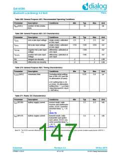
Table 268: General Purpose ADC: Recommended Operating Conditions
Parameter
(ADC)
Description
Conditions
Min
Typ
Max
Unit
N
number of bits (resolu-
tion)
10
bit
BIT
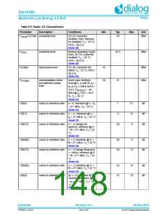
Table 269: General Purpose ADC: DC Characteristics
Parameter Description Conditions
Min
Typ
Max
Unit
V
V
V
V
zero-scale input voltage single-ended, calibrated
at zero input
-2.5
0
2.5
mV
I(ZS)
full-scale input voltage
single-ended, calibrated
at zero input
1150
1180
-1180
1180
1250
mV
mV
mV
I(FS)
negative full-scale input
voltage
differential, calibrated at
zero input
I(FSN)
I(FSP)
positive full-scale input
voltage
differential, calibrated at
zero input
INL
integral non-linearity
-2
-2
2
2
LSB
LSB
DNL
differential non-linearity
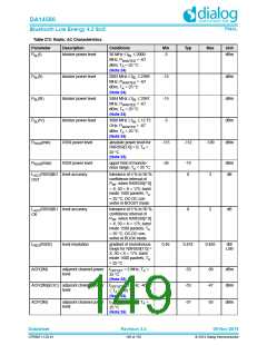
Table 270: General Purpose ADC: Timing Characteristics
Parameter
(ADC)
Description
Conditions
Min
Typ
Max
Unit
t
conversion time
Excluding initial settling
time of the LDO and the
3x-attenuation (if used):
0.25
0.4
s
CONV
LDO settling time is 20
s (max), 3x-attenuation
settling time = 1 s (max)
Using internal ADC-clock
(~200 MHz)
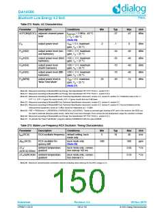
Table 271: Radio: DC Characteristics
Parameter
Description
Conditions
Min
Typ
Max
Unit
I
(RF)RX
battery supply current
receive mode; radio
3.7
4.3
mA
BAT
receiver and synthesizer
active; DCDC converter
assumed ideal; T = 25
A
°C
(Note 19)
I
(RF)TX
battery supply current
transmit mode; radio
transmitter and synthe-
sizer active; DCDC con-
3.4
4
mA
BAT
verter assumed ideal; T
A
= 25 °C
(Note 19)
Note 19: The DCDC-converter efficiency is assumed to be 100 % to enable benchmarking of the radio currents at battery supply domain (VBAT3V =
3 V).
Datasheet
Revision 3.4
09-Nov-2016
CFR0011-120-01
147 of 155
© 2014 Dialog Semiconductor

 DIALOG [ Dialog Semiconductor ]