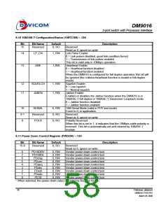
DM9016
3-port switch with Processor Interface
9. Functional Description
9.1 Processor bus and memory management function:
of address is reached.
9.1.1 Processor Interface
When the bit 7 of IMR is cleared, there is a 64K-
byte memory space in the DM9016 can be accessed.
This configured type of internal memory is used for
testing only. The memory write address (register
FAh/FBh) and the memory read address (register
F4h/F5h) represent the physical memory address of
the DM9016 internal memory. It is noted that after the
memory had been written by memory write command,
the switch reset command (bit 6 of register 52h)
should be set before normal switch function operation,
since the controlled data in internal memory may be
corrupted.
In the general processor mode, the chip selection
is just coming from pin 2 (CS#). There are only two
addressing ports through the access of the host
interface.
One port is the INDEX port and the other is the
DATA port. The INDEX port is decoded by the CMD
pin=0 and the DATA by the CMD pin=1. The contents
of the INDEX port are the register address of the
DATA port. Before the access of any register, the
address of the register must be saved in the INDEX
port before.
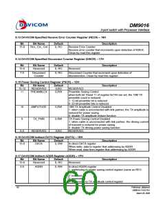
9.1.2 Direct Memory Access Control
The DM9016 provides DMA capability to simplify
the access of the internal memory. After the setting of
the starting address of the internal memory and then
issuing a dummy read/write command to load the
current data to internal data buffer, the desired
location of the internal memory can be accessed by
the read/write command registers. The memory’s
address will be increased with the size equal to the
current operation mode (i.e. the byte, word or
double-word mode) and the data of the next location
will be loaded to internal data buffer automatically. It
is noted that the data of the first access (the dummy
read/write command) in a sequential burst should be
ignored because that the data was the contents of the
last read/write command.
There are two configured types of internal
memory which are controlled by bit 7 of IMR. When
the bit 7 of IMR is set, the internal memory is used for
transmit and receive buffers. The transmit buffer
occupies 7.5K bytes in 3-port mode and 8K bytes in
2-port mode. And the receive buffer occupies 7.5K
bytes in 3-port mode and 7.75K bytes in 2-port mode.
Both the transmit and receive buffer address need
not to be programmed instead that they are managed
by the DM9016 automatically. In transmit function,
after power on reset or each time after the transmit
command is issued (bit 0 of TCR is set), the next
starting transmit buffer address is loaded. In receive
function, the 7.5K-byte (or 7.75K-byte) receive buffer
can be treated as a continued logic memory space.
The memory address will wrap to address 0 if the end
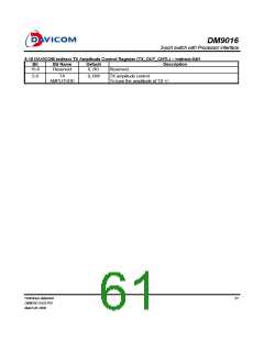
9.1.3 Packet Transmission
There are two packets, sequentially named as
index I and index II, can be stored in the TX SRAM at
the same time. The index register 02h controls the
insertion of CRC.
The start address of transmission is 00h and the
current packet is index I after software or hardware
reset. Firstly write data to the TX SRAM using the
DMA port and then write the byte count to byte count
register at index register 0fch and 0fdh. Set the bit 1
of control register. The DM9016 starts to transmit the
index I packet. Before the transmission of the index I
packet ends, the data of the next (index II) packet can
be moved to TX SRAM. After the index I packet ends
the transmission, write the byte count data of the
index II to BYTE_COUNT register and then set the bit
1 of control register to transmit the index II packet.
The following packets, named index I, II, I, II… use
the same way to be transmitted.
9.1.4 Packet Reception
The RX SRAM is a ring data structure. Each
packet has a 4-byte header followed with the data of
the reception packet which CRC field is included. The
format of the 4-byte header is 01h, status,
BYTE_COUNT low, and BYTE_COUNT high. It is
noted that the start address of each packet is in the
proper address boundary which depends on the
operation mode (byte, word, or double-word mode).
62
Preliminary datasheet
DM9016-13-DS-P01
March 26, 2009

 DAVICOM [ DAVICOM SEMICONDUCTOR, INC. ]