DS3251/DS3252/DS3253/DS3254
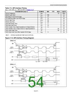
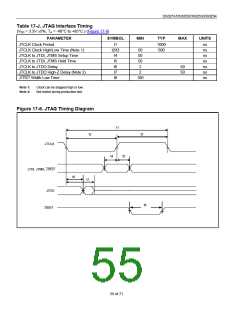
Table 17-J. JTAG Interface Timing
(VDD = 3.3V M5%, TA = -40°C to +85°C.) (Figure 17-6)
PARAMETER
JTCLK Clock Period
JTCLK Clock High/Low Time (Note 1)
JTCLK to JTDI, JTMS Setup Time
JTCLK to JTDI, JTMS Hold Time
JTCLK to JTDO Delay
SYMBOL
MIN
TYP
1000
500
MAX
UNITS
t1
t2/t3
t4
t5
t6
t7
t8
ns
ns
ns
ns
ns
ns
ns
50
50
50
2
2
100
50
50
JTCLK to JTDO High-Z Delay (Note 2)
JTRST Width Low Time
Note 1:
Note 2:
Clock can be stopped high or low.
Not tested during production test.
Figure 17-6. JTAG Timing Diagram
t1
t2
t3
JTCLK
t4
t5
JTDI, JTMS, JTRST
t6
t7
JTDO
55 of 71

 DALLAS [ DALLAS SEMICONDUCTOR ]