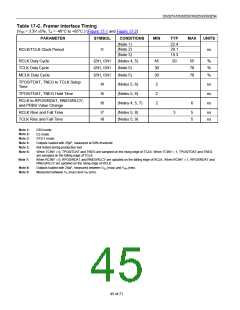
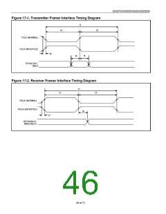
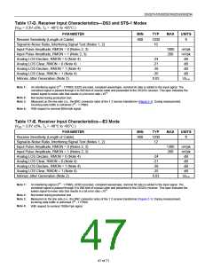
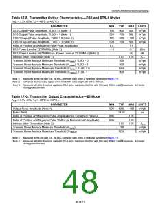
DS3251/DS3252/DS3253/DS3254
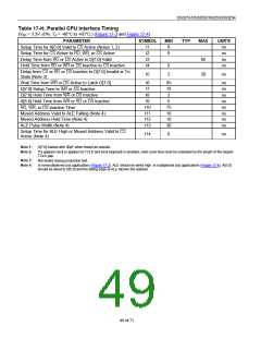
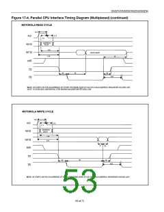
Table 17-H. Parallel CPU Interface Timing
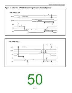
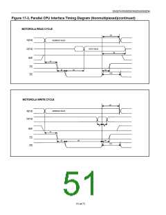
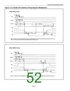
(VDD = 3.3V M5%, TA = -40°C to +85°C.) (Figure 17-3 and Figure 17-4)
PARAMETER
SYMBOL
MIN
0
0
TYP
MAX
UNITS
ns
ns
ns
ns
Setup Time for A[5:0] Valid to CS Active (Notes 1, 2)
Setup Time for CS Active to RD, WR, or DS Active
Delay Time from RD or DS Active to D[7:0] Valid
Hold Time from RD or WR or DS Inactive to CS Inactive
t1
t2
t3
t4
65
20
0
2
Delay from CS or RD or DS Inactive to D[7:0] Invalid or Tri-
t5
ns
State (Note 3)
Wait Time from WR or DS Active to Latch D[7:0]
D[7:0] Setup Time to WR or DS Inactive
D[7:0] Hold Time from WR or DS Inactive
A[5:0] Hold Time from WR or RD or DS Inactive
RD, WR, or DS Inactive Time
Muxed Address Valid to ALE Falling (Note 4)
Muxed Address Hold Time (Note 4)
ALE Pulse Width (Note 4)
t6
t7
t8
65
10
2
ns
ns
ns
ns
ns
ns
ns
ns
t9
5
t10
t11
t12
t13
75
10
10
30
Setup Time for ALE High or Muxed Address Valid to CS
t14
0
ns
Active (Note 4)
Note 1:
Note 2:
D[7:0] loaded with 50pF when tested as outputs.
If a gapped clock is applied on TCLK and local loopback is enabled, read cycle time must be extended by the length of the largest
TCLK gap.
Not tested during production test.
Note 3:
Note 4:
In nonmultiplexed bus applications (Figure 17-3), ALE should be wired high. In multiplexed bus applications (Figure 17-4), A[5:0]
should be wired to D[5:0] and the falling edge of ALE latches the address.
49 of 71

 DALLAS [ DALLAS SEMICONDUCTOR ]