DS3251/DS3252/DS3253/DS3254
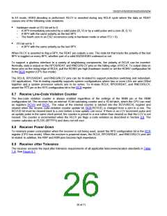
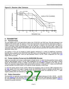
Figure 8-1. Receiver Jitter Tolerance
15
STS-1 GR253
DS3 GR-499 Cat II
DS3 GR-499 Cat I
10
5
10
DS325x JITTER TOLERANCE
1.5
E3 G.823
1.0
0.1
0.3
0.15
0.1
30
300
669
2.3k
22.3k
60k
300k 800k
10
100
1k
10k
100k
1M
FREQUENCY (Hz)
9. TRANSMITTER
9.1 Transmit Clock
The clock applied at the TCLK input clocks in data on the TPOS/TDAT and TNEG pins. If the jitter attenuator is not
enabled in the transmit path, the signal on TCLK is the transmit line clock and must be transmission quality (i.e.,
M20ppm frequency accuracy and low jitter). If the jitter attenuator is enabled in the transmit path, the signal on
TCLK can be jittery and/or periodically gapped, but must still have an average frequency within M20ppm of the
nominal line rate. When enabled in the transmit path, the jitter attenuator generates the transmit line clock from the
appropriate master clock.
The polarity of TCLK can be inverted to support glueless interfacing to a variety of neighboring components.
Normally data is sampled on the TPOS/TDAT and TNEG pins on the rising edge of TCLK. To sample data on the
falling edge of TCLK, pull the TCINV pin high (hardware mode) or set the TCINV configuration bit in the TCR
register (CPU bus mode).
9.2 Framer Interface Format and the B3ZS/HDB3 Encoder
Data to be transmitted can be input in either binary or bipolar format. To select the binary interface format, pull the
TBIN pin high (hardware mode) or set the TBIN configuration bit in the TCR register (CPU bus mode). In binary
format, the B3ZS/HBD3 encoder is enabled, and the data to be transmitted is sampled on the TDAT pin. The
TNEG pin is ignored in binary interface mode and should be wired low. In DS3 and STS-1 modes, the B3ZS/HDB3
encoder operates in the B3ZS mode. In E3 mode the encoder operates in HDB3 mode.
To select the bipolar interface format, pull the TBIN pin low (hardware mode) or clear the TBIN configuration bit in
the TCR register (CPU bus mode). In bipolar format, the B3ZS/HDB3 encoder is disabled and the data to be
transmitted is sampled on the TPOS and TNEG pins. Positive-polarity pulses are indicated by TPOS = 1, while
negative-polarity pulses are indicated by TNEG = 1.
9.3 Pattern Generation
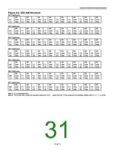
The transmitter can generate several patterns internally, including unframed all ones (E3 AIS), 100100…, and DS3
AIS. See Figure 9-2 for the structure of the DS3 AIS signal. The TDSA and TDSB input pins (hardware mode) or
the TDSA and TDSB control bits in the GCR register (CPU bus mode) are used to select these patterns. Table 6-G
indicates the possible selections.
27 of 71

 DALLAS [ DALLAS SEMICONDUCTOR ]