DS3251/DS3252/DS3253/DS3254
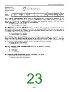
Register Name:
CACR
Register Description:
Register Address:
Clock Adapter Control Register
08h
Bit
7
T3MOE
0
6
E3MOE
0
5
STMOE
0
4
—
0
3
—
0
2
1
0
Name
Default
AMCSEL[1] AMCSEL[0] AMCEN
0
0
0
Bit 7: T3MCLK Output Enable (T3MOE). When the clock adapter block is configured to synthesize the DS3
master clock, the DS3 master clock can be output on the T3MCLK pin by setting T3MOE=1. This clock can then be
used as the transmit clock for neighboring DS3 framers and other components requiring a DS3 clock. This bit
should only be set to 1 if the T3MCLK pin is not driven externally.
0 = T3MCLK output driver disabled
1 = T3MCLK output driver enabled
Bit 6: E3MCLK Output Enable (E3MOE). When the clock adapter block is configured to synthesize the E3 master
clock, the E3 master clock can be output on the E3MCLK pin by setting E3MOE=1. This clock can then be used as
the transmit clock for neighboring E3 framers and other components requiring an E3 clock. This bit should only be
set to 1 if the E3MCLK pin is not driven externally.
0 = E3MCLK output driver disabled
1 = E3MCLK output driver enabled
Bit 5: STMCLK Output Enable (STMOE). When the clock adapter block is configured to synthesize the STS-1
master clock, the STS-1 master clock can be output on the of the STMCLK pin by setting STMOE=1. This clock
can then be used as the transmit clock for neighboring SONET framers, mappers and other components requiring
an STS-1 clock. This bit should only be set to 1 if the STMCLK pin is not driven externally.
0 = STMCLK output driver disabled
1 = STMCLK output driver enabled
Bits 2 to 1: Alternate Master Clock Select (AMCSEL[1:0]). See Section 12 for details.
00 = 19.44 MHz
01 = 38.88 MHz
10 = 77.76 MHz
11 = {unused value}
Bit 0: Alternate Master Clock Enable (AMCEN). See Section 12 for details.
0 = alternate master clock mode disabled
1 = alternate master clock mode enabled
23 of 71

 DALLAS [ DALLAS SEMICONDUCTOR ]