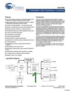
SL811HS
Table 1. SL811HS Master (Host) Mode Registers
USB Transceiver
The SL811HS has a built in transceiver that meets USB Specifi-
cation 1.1. The transceiver is capable of transmitting and
receiving serial data at USB full speed (12 Mbits) and low speed
(1.5 Mbits). The driver portion of the transceiver is differential
while the receiver section is comprised of a differential receiver
and two single-ended receivers. Internally, the transceiver inter-
faces to the Serial Interface Engine (SIE) logic. Externally, the
transceiver connects to the physical layer of the USB.
Register Name
SL811HS
SL811HS
(hex) Address
USB-A Host Control Register
USB-A Host Base Address
USB-A Host Base Length
00h
01h
02h
03h
USB-A Host PID, Device Endpoint
(Write)/USB Status (Read)
USB-A Host Device Address
(Write)/Transfer Count (Read)
04h
SL811HS Registers
Operation and control of the SL811HS is managed through
internal registers. When operating in Master/Host mode, the first
16 address locations are defined as register space. In
Slave/Peripheral mode, the first 64 bytes are defined as register
space. The register definitions vary greatly between each mode
of operation and are defined separately in this document (section
“Table 1 shows the memory map and register mapping of the
SL811HS in master/host mode.” on page 5 describes Host
register definitions, while section “SL811HS Slave Mode
Registers” on page 14 describes Slave register definitions).
Access to the registers are through the microprocessor interface
similar to normal RAM accesses (see “Bus Interface Timing
Requirements” on page 25) and provide control and status infor-
mation for USB transactions.
Control Register 1
05h
Interrupt Enable Register
Reserved Register
06h
Reserved
08h
USB-B Host Control Register
USB-B Host Base Address
USB-B Host Base Length
09h
0Ah
USB-B Host PID, Device Endpoint
(Write)/USB Status (Read)
0Bh
USB-B Host Device Address
(Write)/Transfer Count (Read)
0Ch
0Dh
Status Register
Any write to control register 0FH enables the SL811HS full
features bit. This is an internal bit of the SL811HS that enables
additional features.
SOF Counter LOW (Write)/HW Revision 0Eh
Register (Read)
SOF Counter HIGH and Control Register 2 0Fh
Table 1 shows the memory map and register mapping of the
SL811HS in master/host mode.
Memory Buffer
10H-FFh
The registers in the SL811HS are divided into two major groups.
The first group is referred to as USB Control registers. These
registers enable and provide status for control of USB transac-
tions and data flow. The second group of registers provides
control and status for all other operations.
Register Values on Power-up and Reset
The following registers initialize to zero on power-up and reset:
■ USB-A/USB-B Host Control Register [00H, 08H] bit 0 only
■ Control Register 1 [05H]
■ USB Address Register [07H]
■ Current Data Set/Hardware Revision/SOF Counter LOW
Register [0EH]
All other register’s power-up and reset in an unknown state and
firmware for initialization.
Document 38-08008 Rev. *F
Page 5 of 32
[+] Feedback

 CYPRESS [ CYPRESS ]