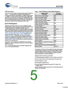
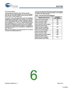
SL811HS
Figure 3. Optional 12 MHz Crystal Circuit
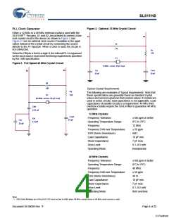
PLL Clock Generator
Either a 12 MHz or a 48 MHz external crystal is used with the
SL811HS[1]. Two pins, X1 and X2, are provided to connect a low
cost crystal circuit to the device as shown in Figure 2 and
Figure 2. Use an external clock source if available in the appli-
cation instead of the crystal circuit by connecting the source
directly to the X1 input pin. When a clock is used, the X2 pin is
not connected.
X1
X2
Rf
1M
Rs
100
When the CM pin is tied to a logic 0, the internal PLL is bypassed
so the clock source must meet the timing requirements specified
by the USB specification.
X1
Figure 2. Full Speed 48 MHz Crystal Circuit
12 MHz , series, 20-pF load
X2
Cin
Cout
X1
22 pF
22 pF
Rf
1M
Typical Crystal Requirements
Rs
The following are examples of ‘typical requirements.’ Note that
these specifications are generally found as standard crystal
values and are less expensive than custom values. If crystals are
used in series circuits, load capacitance is not applicable. Load
capacitance of parallel circuits is a requirement. 48 MHz third
overtone crystals require the Cin/Lin filter to guarantee 48 MHz
operation.
X1
100
48 MHz, series, 20-pF load
Cbk
0.01 μF
12 MHz Crystals:
Cout
Frequency Tolerance:
Operating Temperature Range:
Frequency:
±100 ppm or better
0°C to 70°C
12 MHz
Lin
22 pF
Cin
2.2 μH
22 pF
Frequency Drift over Temperature:
ESR (Series Resistance):
Load Capacitance:
± 50 ppm
60Ω
10 pF min.
7 pF max.
0.1–0.5 mW
fundamental
Shunt Capacitance:
Drive Level:
Operating Mode:
48 MHz Crystals:
Frequency Tolerance:
Operating Temperature Range:
Frequency:
±100 ppm or better
0°C to 70°C
48 MHz
Frequency Drift over Temperature:
ESR (Series Resistance):
Load Capacitance:
± 50 ppm
40 Ω
10 pF min.
7 pF max.
Shunt Capacitance:
Drive Level:
0.1–0.5 mW
third overtone
Operating Mode:
Note
1. CM (Clock Multiply) pin of the SL811HS must be tied to GND when 48 MHz crystal circuit or 48 MHz clock source is used.
Document 38-08008 Rev. *F
Page 4 of 32
[+] Feedback

 CYPRESS [ CYPRESS ]