CY8C27x43 Final Data Sheet
1. Pin Information
1.1.5
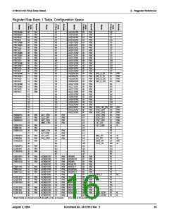
48-Pin Part Pinouts
Table 1-5. 48-Pin Part Pinout (SSOP)
Type
CY8C27643 48-Pin PSoC Device
Pin
No.
Pin
Name
Description
Digital Analog
1
IO
IO
IO
IO
IO
IO
IO
IO
IO
IO
IO
IO
I
P0[7]
P0[5]
P0[3]
P0[1]
P2[7]
P2[5]
P2[3]
P2[1]
P4[7]
P4[5]
P4[3]
P4[1]
SMP
Analog column mux input.
AI, P0[7]
1
2
Vdd
48
47
46
45
44
43
42
41
40
39
38
37
36
35
34
33
32
31
30
29
28
27
26
25
AIO, P0[5]
AIO, P0[3]
2
IO
IO
I
Analog column mux input and column output.
Analog column mux input and column output.
Analog column mux input.
P0[6], AI
P0[2], AIO
P0[4], AIO
P0[0], AI
P2[6], External VRef
P2[4], External AGND
P2[2], AI
P2[0], AI
P4[6]
3
4
5
3
AI, P0[1]
P2[7]
4
5
P2[5]
6
7
6
AI, P2[3]
AI, P2[1]
P4[7]
7
I
I
Direct switched capacitor block input.
Direct switched capacitor block input.
8
9
10
8
P4[5]
9
P4[3]
11
12
13
14
15
16
P4[4]
P4[2]
10
11
12
13
P4[1]
SSOP
SMP
P4[0]
P3[7]
XRES
Power
Power
Input
Switch Mode Pump (SMP) connection to
external components required.
P3[5]
P3[6]
P3[3]
P3[1]
P3[4]
14
15
16
17
18
19
20
21
22
23
24
25
IO
IO
IO
IO
IO
IO
IO
IO
IO
IO
P3[7]
P3[5]
P3[3]
P3[1]
P5[3]
P5[1]
P1[7]
P1[5]
P1[3]
P1[1]
Vss
17
18
19
20
21
P3[2]
P5[3]
P5[1]
I2C SCL, P1[7]
P3[0]
P5[2]
P5[0]
P1[6]
I2C SDA, P1[5]
P1[3]
I2C SCL, XTALin, P1[1]
Vss
22
23
24
P1[4], EXTCLK
P1[2]
I2C Serial Clock (SCL)
I2C Serial Data (SDA)
P1[0], XTALout, I2C SDA
Crystal Input (XTALin), I2C Serial Clock (SCL)
Ground connection.
IO
P1[0]
Crystal Output (XTALout), I2C Serial Data
(SDA)
26
27
28
29
30
31
32
33
34
35
IO
IO
IO
IO
IO
IO
IO
IO
IO
P1[2]
P1[4]
P1[6]
P5[0]
P5[2]
P3[0]
P3[2]
P3[4]
P3[6]
XRES
Optional External Clock Input (EXTCLK)
Active high external reset with internal pull
down.
36
37
38
39
40
41
42
43
44
45
46
47
48
IO
IO
IO
IO
IO
IO
IO
IO
IO
IO
IO
IO
P4[0]
P4[2]
P4[4]
P4[6]
P2[0]
P2[2]
P2[4]
P2[6]
P0[0]
P0[2]
P0[4]
P0[6]
Vdd
I
I
Direct switched capacitor block input.
Direct switched capacitor block input.
External Analog Ground (AGND)
External Voltage Reference (VRef)
Analog column mux input.
I
IO
IO
I
Analog column mux input and column output.
Analog column mux input and column output.
Analog column mux input.
Power
Supply voltage.
LEGEND: A = Analog, I = Input, and O = Output.
August 3, 2004
Document No. 38-12012 Rev. *I
12

 CYPRESS [ CYPRESS ]