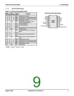
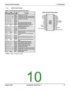
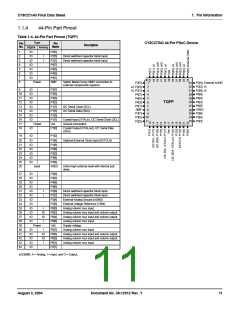
1. Pin Information
This chapter describes, lists, and illustrates the CY8C27x43 PSoC device pins and pinout configurations.
1.1
Pinouts
The CY8C27x43 PSoC device is available in a variety of packages which are listed and illustrated in the following tables. Every port
pin (labeled with a “P”) is capable of Digital IO. However, Vss, Vdd, SMP, and XRES are not capable of Digital IO.
1.1.1
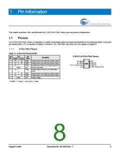
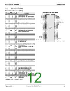
8-Pin Part Pinout
Table 1-1. 8-Pin Part Pinout (PDIP)
Type
CY8C27143 8-Pin PSoC Device
Pin
No.
Pin
Name
Description
Digital Analog
1
2
3
4
5
IO
IO
IO
IO
IO
P0[5]
Analog column mux input and column output.
Analog column mux input and column output.
Crystal Input (XTALin), I2C Serial Clock (SCL)
Ground connection.
Vdd
AIO, P0[5]
AIO, P0[3]
1
2
3
4
8
7
6
5
P0[4], AIO
P0[3]
P1[1]
Vss
PDIP
P0[2], AIO
I2C SCL, XTALin, P1[1]
Vss
P1[0], XTALout, I2C SDA
Power
IO
P1[0]
Crystal Output (XTALout), I2C Serial Data
(SDA)
6
7
8
IO
IO
IO
IO
P0[2]
P0[4]
Vdd
Analog column mux input and column output.
Analog column mux input and column output.
Supply voltage.
Power
LEGEND: A = Analog, I = Input, and O = Output.
August 3, 2004
Document No. 38-12012 Rev. *I
8

 CYPRESS [ CYPRESS ]