CY8C27x43 Final Data Sheet
1. Pin Information
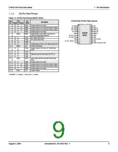
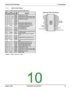
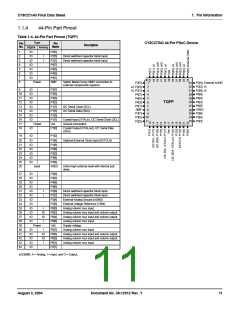
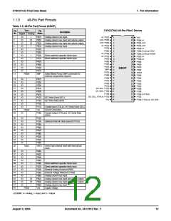
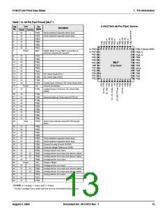
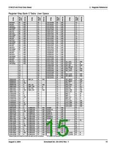
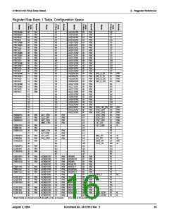
Table 1-6. 48-Pin Part Pinout (MLF*)
Type
CY8C27643 48-Pin PSoC Device
Pin
No.
Pin
Name
Description
Digital Analog
1
2
3
4
5
6
7
IO
IO
IO
IO
IO
IO
I
I
P2[3]
P2[1]
P4[7]
P4[5]
P4[3]
P4[1]
SMP
Direct switched capacitor block input.
Direct switched capacitor block input.
P2[4], External AGND
P2[2], AI
AI, P2[3]
AI, P2[1]
P4[7]
36
35
34
33
32
31
1
2
Power
Power
Input
Switch Mode Pump (SMP) connection to
external components required.
3
4
5
6
P2[0], AI
P4[6]
8
IO
IO
IO
IO
IO
IO
IO
IO
IO
IO
P3[7]
P3[5]
P3[3]
P3[1]
P5[3]
P5[1]
P1[7]
P1[5]
P1[3]
P1[1]
Vss
P4[5]
P4[3]
P4[1]
SMP
P3[7]
P3[5]
P3[3]
P3[1]
P5[3]
9
P4[4]
10
11
12
13
14
15
16
17
18
19
P4[2]
MLF
(Top View)
30
29
28
27
P4[0]
7
8
9
XRES
P3[6]
P3[4]
10
I2C Serial Clock (SCL)
I2C Serial Data (SDA)
26
25
P3[2]
P3[0]
11
12
Crystal Input (XTALin), I2C Serial Clock (SCL)
Ground connection.
IO
P1[0]
Crystal Output (XTALout), I2C Serial Data
(SDA)
20
21
22
23
24
25
26
27
28
29
IO
IO
IO
IO
IO
IO
IO
IO
IO
P1[2]
P1[4]
P1[6]
P5[0]
P5[2]
P3[0]
P3[2]
P3[4]
P3[6]
XRES
Optional External Clock Input (EXTCLK)
Active high external reset with internal pull
down.
30
31
32
33
34
35
36
37
38
39
40
41
42
43
44
45
46
47
48
IO
IO
IO
IO
IO
IO
IO
IO
IO
IO
IO
IO
P4[0]
P4[2]
P4[4]
P4[6]
P2[0]
P2[2]
P2[4]
P2[6]
P0[0]
P0[2]
P0[4]
P0[6]
Vdd
I
I
Direct switched capacitor block input.
Direct switched capacitor block input.
External Analog Ground (AGND)
External Voltage Reference (VRef)
Analog column mux input.
I
IO
IO
I
Analog column mux input and column output.
Analog column mux input and column output.
Analog column mux input.
Power
Supply voltage.
IO
IO
IO
IO
IO
IO
I
P0[7]
P0[5]
P0[3]
P0[1]
P2[7]
P2[5]
Analog column mux input.
IO
IO
I
Analog column mux input and column output.
Analog column mux input and column output.
Analog column mux input.
LEGEND: A = Analog, I = Input, and O = Output.
* The MLF package has a center pad that must be connected to ground (Vss).
August 3, 2004
Document No. 38-12012 Rev. *I
13

 CYPRESS [ CYPRESS ]