CY7C68013A, CY7C68014A
CY7C68015A, CY7C68016A
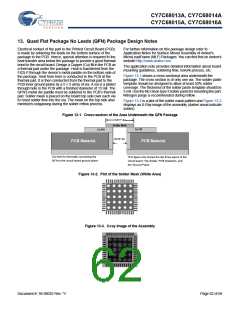
13. Quad Flat Package No Leads (QFN) Package Design Notes
Electrical contact of the part to the Printed Circuit Board (PCB)
is made by soldering the leads on the bottom surface of the
package to the PCB. Hence, special attention is required to the
heat transfer area below the package to provide a good thermal
bond to the circuit board. Design a Copper (Cu) fill in the PCB as
a thermal pad under the package. Heat is transferred from the
FX2LP through the device’s metal paddle on the bottom side of
the package. Heat from here is conducted to the PCB at the
thermal pad. It is then conducted from the thermal pad to the
PCB inner ground plane by a 5 × 5 array of via. A via is a plated
through hole in the PCB with a finished diameter of 13 mil. The
QFN’s metal die paddle must be soldered to the PCB’s thermal
pad. Solder mask is placed on the board top side over each via
to resist solder flow into the via. The mask on the top side also
minimizes outgassing during the solder reflow process.
For further information on this package design refer to
Application Notes for Surface Mount Assembly of Amkor's
MicroLeadFrame (MLF) Packages. You can find this on Amkor's
website http://www.amkor.com.
The application note provides detailed information about board
mounting guidelines, soldering flow, rework process, etc.
Figure 13-1 shows a cross-sectional area underneath the
package. The cross section is of only one via. The solder paste
template should be designed to allow at least 50% solder
coverage. The thickness of the solder paste template should be
5 mil. Use the No Clean type 3 solder paste for mounting the part.
Nitrogen purge is recommended during reflow.
Figure 13-2 is a plot of the solder mask pattern and Figure 13-3
displays an X-Ray image of the assembly (darker areas indicate
solder).
Figure 13-1. Cross-section of the Area Underneath the QFN Package
0.017” dia
Solder Mask
Cu Fill
Cu Fill
0.013” dia
PCB Material
PCB Material
Via hole for thermally connecting the
This figure only shows the top three layers of the
circuit board: Top Solder, PCB Dielectric, and
the Ground Plane
QFN to the circuit board ground plane.
Figure 13-2. Plot of the Solder Mask (White Area)
Figure 13-3. X-ray Image of the Assembly
Document #: 38-08032 Rev. *V
Page 62 of 66

 CYPRESS [ CYPRESS ]