CY7C68013A, CY7C68014A
CY7C68015A, CY7C68016A
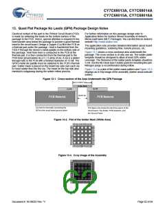
12. PCB Layout Recommendations
Follow these recommendations to ensure reliable high
performance operation:[25]
■ Bypass and flyback caps on VBus, near connector, are
recommended.
■ Four layer impedance controlled boards are required to
maintain signal quality.
■ DPLUS and DMINUS trace lengths should be kept to within
2 mm of each other in length, with preferred length of 20 to
30 mm.
■ Specify impedance targets (ask your board vendor what they
can achieve).
■ Maintain a solid ground plane under the DPLUS and DMINUS
traces. Do not allow the plane to split under these traces.
■ To control impedance, maintain trace widths and trace spacing.
■ Minimize stubs to minimize reflected signals.
■ Do not place vias on the DPLUS or DMINUS trace routing.
■ Isolate the DPLUS and DMINUS traces from all other signal
traces by no less than 10 mm.
■ Connections between the USB connector shell and signal
ground must be near the USB connector.
Note
25. Source for recommendations: EZ-USB FX2™PCB Design Recommendations, http://www.cypress.com and High Speed USB Platform Design Guidelines,
http://www.usb.org/developers/docs/hs_usb_pdg_r1_0.pdf.
Document #: 38-08032 Rev. *V
Page 61 of 66

 CYPRESS [ CYPRESS ]