FOR
FOR
CY7C63411/12/13
CY7C63511/12/13
CY7C63612/13
LIST OF FIGURES
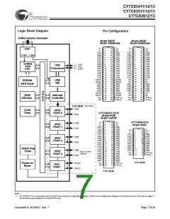
Figure 6-1. Program Memory Space with Interrupt Vector Table ......................................................... 12
Figure 7-1. Clock Oscillator On-chip Circuit .......................................................................................... 15
Figure 8-1. Watch Dog Reset (WDR) ................................................................................................... 16
Figure 9-1. Block Diagram of a GPIO Line ........................................................................................... 16
Figure 9-2. Port 1 Data 0x01h (read/write) ........................................................................................... 17
Figure 9-3. Port 2 Data 0x02h (read/write) ........................................................................................... 17
Figure 9-4. Port 3 Data 0x03h (read/write) ........................................................................................... 17
Figure 9-5. DAC Port Data 0x30h (read/write) ...................................................................................... 17
Figure 9-6. Port 0 Interrupt Enable 0x04h (write only) .......................................................................... 17
Figure 9-7. Port 1 Interrupt Enable 0x05h (write only) .......................................................................... 17
Figure 9-8. Port 2 Interrupt Enable 0x06h (write only) .......................................................................... 17
Figure 9-9. Port 3 Interrupt Enable 0x07h (write only) .......................................................................... 17
Figure 10-1. Block Diagram of DAC Port .............................................................................................. 19
Figure 10-2. DAC Port Data 0x30h (read/write) .................................................................................... 19
Figure 10-3. DAC Port Interrupt Enable 0x31h (write only) .................................................................. 19
Figure 10-4. DAC Port Interrupt Polarity 0x32h (write only) ................................................................. 19
Figure 10-5. DAC Port Isink 0x38h to 0x3Fh (write only) ..................................................................... 20
Figure 11-1. USB Status and Control Register 0x1Fh .......................................................................... 21
Figure 12-1. USB Device Address Register 0x10h (read/write) ........................................................... 21
Figure 12-2. USB Device Counter Registers 0x11h, 0x13h, 0x15h (read/write) .................................. 22
Figure 13-1. Timer Block Diagram ........................................................................................................ 23
Figure 15-1. USB End Point Interrupt Enable Register 0x21h (read/write) .......................................... 24
Figure 19-1. Clock Timing ..................................................................................................................... 32
Figure 19-2. USB Data Signal Timing ................................................................................................... 32
Figure 19-3. Receiver Jitter Tolerance ................................................................................................. 32
Figure 19-4. Differential to EOP Transition Skew and EOP Width ....................................................... 33
Figure 19-5. Differential Data Jitter ....................................................................................................... 33
LIST OF TABLES
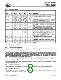
Table 6-1. I/O Register Summary ........................................................................................................14
Table 15-1. Interrupt Vector Assignments ...........................................................................................24
Table 16-1. USB Register Mode Encoding ..........................................................................................26
Table 16-2. Decode table forTable 16-3: “Details of Modes for Differing Traffic Conditions” ..............27
Table 16-3. Details of Modes for Differing Traffic Conditions ..............................................................28
Document #: 38-08027 Rev. **
Page 4 of 36

 CYPRESS [ CYPRESS ]