FOR
FOR
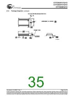
CY7C63411/12/13
CY7C63511/12/13
CY7C63612/13
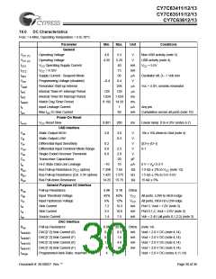
Parameter
Min.
Max.
0.5
0.8
21
Unit
lsb
Conditions
Ilin
Differential Nonlinearity
Any pin (note 8,14)
tsink
Tratio
Current Sink Response Time
µs
Full scale transition (note 14)
Vout = 2.0V (note 9,14)
Tracking Ratio DAC[1:0] to DAC[7:2]
14
19.0
Switching Characteristics
Parameter
Description
Clock
Min.
Max.
Unit
Conditions
tCYC
tCH
tCL
Input Clock Cycle Time
Clock HIGH Time
165.0
168.3
ns
ns
ns
0.45 tCYC
0.45 tCYC
Clock LOW Time
USB Driver Characteristics
Transition Rise Time
tr
75
75
ns
ns
ns
ns
%
V
CLoad = 50 pF [4, 5]
CLoad = 600 pF [4, 5]
CLoad = 50 pF [4, 5]
CLoad = 600 pF [4, 5]
tr
Transition Rise Time
300
tf
Transition Fall Time
tf
Transition Fall Time
300
125
2.0
[4, 5]
trfm
Vcrs
Rise/Fall Time Matching
Output Signal Crossover Voltage
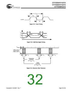
USB Data Timing
80
tr/tf
[4, 5]
1.3
tdrate
tdjr1
Low Speed Data Rate
Receiver Data Jitter Tolerance
Receiver Data Jitter Tolerance
Differential toEOP Transition Skew
EOP Width at Receiver
EOP Width at Receiver
Source EOP Width
1.4775
–75
1.5225
75
Mbs
ns
ns
ns
ns
ns
µs
ns
ns
Ave. Bit Rate (1.5 Mb/s ± 1.5%)
To Next Transition [12]
For Paired Transitions [12]
tdjr2
–45
45
[10]
tdeop
teopr1
teopr2
teopt
tudj1
tudj2
–40
100
330
Rejects as EOP [12]
Accepts as EOP [12]
675
1.25
–95
1.50
95
Differential Driver Jitter
Differential Driver Jitter
To next transition, Figure 19-5
To paired transition, Figure 19-5
–150
150
Notes:
3. Functionality is guaranteed of the VCC (1) range, except USB transmitter and DACs.
4. USB transmitter functionality is guaranteed over the VCC (2) range, as well as DAC outputs.
5. Per Table 7-7 of revision 1.1 of USB specification, for CLOAD of 50–600 pF.
6. Port 3 bit 7 controls whether the parts goes into suspend after a POR event or waits 128 ms to begin running.
7. POR will re-occur whenever VCC drops to approximately 2.5V.
8. Measured as largest step size vs. nominal according to measured full scale and zero programmed values.
9.
Tratio = Isink1[1:0](n)/Isink0[7:2](n) for the same n, programmed.
10. Total current cumulative across all Port pins flowing to VSS is limited to minimize Ground-Drop noise effects.
11. Irange: Isinkn(15)/ Isinkn(0) for the same pin.
12. Measured at crossover point of differential data signals.
13. Limits total bus capacitance loading (CLOAD) to 400 pF per section 7.1.5 of revision 1.1 of USB specification.
14. DAC I/O Port not bonded out on CY7C63612/13. See note on page 17 for firmware code needed for unused pins.
Document #: 38-08027 Rev. **
Page 31 of 36

 CYPRESS [ CYPRESS ]