FOR
FOR
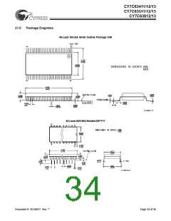
CY7C63411/12/13
CY7C63511/12/13
CY7C63612/13
18.0
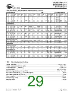
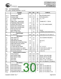
DC Characteristics
Fosc = 6 MHz; Operating Temperature = 0 to 70°C
Parameter
General
Min.
Max.
Unit
Conditions
VCC (1)
VCC (2)
ICC1
ICC2
ISB1
VPP
Tstart
tint1
Operating Voltage
4.0
5.5
5.25
40
V
V
Non USB activity (note 3)
Operating Voltage
4.35
USB activity (note 4)
VCC = 5.5V
VCC Operating Supply Current
VCC = 4.35V
mA
mA
µA
V
15
Supply Current - Suspend Mode
Programming Voltage (disabled)
Resonator Start-up Interval
Internal Timer #1 Interrupt Period
Internal Timer #2 Interrupt Period
Watch Dog Timer Period
Input Leakage Current
Max ISS IO Sink Current
Power-On Reset
30
Oscillator off, D– > Voh min
–0.4
0.4
256
128
µs
µs
ms
ms
µA
mA
Vcc = 5.0V, ceramic resonator
128
tint2
1.024 1.024
twatch
Iil
8.192 14.33
1
Any pin
Ism
60
Cumulative across all ports (note 10)
tvccs
VCC Reset Slew
0.001
2.8
200
ms
Linear ramp: 0 to 4.35V (notes 6,7)
15k ± 5% ohms to Gnd (note 4)
USB Interface
Voh
Vol
Static Output HIGH
3.6
0.3
V
V
Static Output LOW
Vdi
Differential Input Sensitivity
Differential Input Common Mode Range
Single-Ended Receiver Threshold
Transceiver Capacitance
Hi-Z State Data Line Leakage
Bus Pull-up Resistance (VCC option)
Bus Pull-up Resistance (Ext. 3.3V option)
Bus Pull-down Resistance
General Purpose I/O Interface
Pull-up Resistance
0.2
0.8
0.8
V
|(D+)–(D–)|
Vcm
Vse
Cin
Ilo
2.5
2.0
20
V
9-1
V
pF
µA
kΩ
kΩ
kΩ
–10
10
0 V < Vin<3.3 V
Rpu
Rpu
Rpd
7.35K
7.65
7.5 kΩ ± 2% to VCC (note 13)
1.5 kΩ ± 5% to 3.0–3.6V
15 kΩ ± 5%
1.425 1.575
14.25 15.75
Rup
Vith
VH
Iol
4.9K
45%
6%
9.1K
65%
12%
16.5
10.6
7.5
Ohms
VCC
VCC
mA
Input Threshold Voltage
Input Hysteresis Voltage
Sink Current
All ports, LOW to HIGH edge
All ports, HIGH to LOW edge
Port 3, Vout = 1.0V (note 3)
7.2
Iol
Sink Current
3.5
mA
Port 0,1,2, Vout = 2.0V (note 3)
Voh = 2.4V (all ports 0,1,2,3) (note 3)
Ioh
Source Current
1.4
mA
DAC Interface
Rup
Pull-up Resistance
8.0K
0.1
0.5
1.6
8
20.0K
0.3
1.5
4.8
24
Ohms (note 14)
Isink0(0)
Isink0(F)
Isink1(0)
Isink1(F)
Irange
DAC[7:2] Sink Current (0)
DAC[7:2] Sink Current (F)
DAC[1:0] Sink Current (0)
DAC[1:0] Sink Current (F)
Programmed Isink Ratio: max/min
mA
mA
mA
mA
Vout = 2.0 V DC (note 4,14)
Vout = 2.0 V DC (note 4,14)
Vout = 2.0 V DC (note 4,14)
Vout = 2.0 V DC (note 4,14)
Vout = 2.0 V DC (notes 4,11,14)
4
6
Document #: 38-08027 Rev. **
Page 30 of 36

 CYPRESS [ CYPRESS ]