CY7C1361B
CY7C1363B
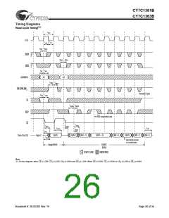
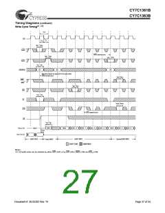
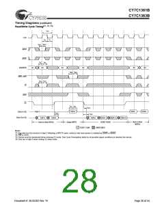
Timing Diagrams (continued)
Read/Write Cycle Timing[21, 23, 24]
t
CYC
CLK
t
t
CL
CH
t
t
ADH
ADS
ADSP
ADSC
t
t
AH
AS
A1
A2
A3
A4
A5
A6
ADDRESS
t
t
WEH
WES
BWE, BW
X
t
t
CEH
CES
CE
ADV
OE
t
t
DH
DS
t
OELZ
t
High-Z
D(A3)
D(A5)
D(A6)
Data In (D)
t
OEHZ
CDV
Data Out (Q)
Q(A1)
Q(A2)
Q(A4)
Q(A4+1)
Q(A4+2)
Q(A4+3)
Back-to-Back
Back-to-Back READs
Single WRITE
BURST READ
WRITEs
DON’T CARE
UNDEFINED
Notes:
23.
24.
.
The data bus (Q) remains in high-Z following a WRITE cycle, unless a new read access is initiated by
GW is HIGH.
ADSP or ADSC
25. Device must be deselected when entering ZZ mode. See Cycle Descriptions table for all possible signal conditions to deselect the device.
26. DQs are in high-Z when exiting ZZ sleep mode.
Document #: 38-05302 Rev. *B
Page 28 of 34

 CYPRESS [ CYPRESS ]