PRELIMINARY
CY7C1061AV25
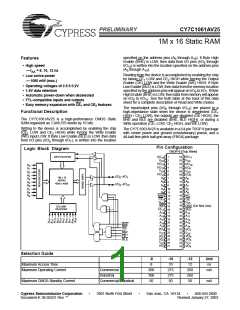
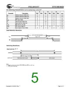
AC Test Loads and Waveforms[3]
R1 1667 Ω
50Ω
2.5V
OUTPUT
= V /2
VTH
DD
OUTPUT
Z = 50Ω
30 pF*
0
R2
1538Ω
5 pF*
INCLUDING
JIG AND
SCOPE
(a)
* Capacitive Load consists of all com-
ponents of the test environment.
(b)
ALL INPUT PULSES
90%
10%
2.5V
90%
10%
GND
Fall time:
> 1V/ns
Rise time > 1V/ns
(c)
AC Switching Characteristics Over the Operating Range [4]
-8
-10
-12
Parameter
Read Cycle
tpower
tRC
Description
Min.
Max.
Min.
Max.
Min.
Max.
Unit
VCC(typical) to the first access[5]
Read Cycle Time
1
8
1
1
ms
ns
ns
ns
ns
ns
ns
ns
ns
ns
ns
ns
ns
ns
ns
10
12
tAA
Address to Data Valid
8
10
12
tOHA
Data Hold from Address Change
CE1 LOW/CE2 HIGH to Data Valid
OE LOW to Data Valid
3
3
3
tACE
8
5
10
5
12
6
tDOE
tLZOE
OE LOW to Low-Z
OE HIGH to High-Z[6]
1
3
0
1
3
0
1
3
0
tHZOE
tLZCE
5
5
5
5
6
6
CE1 LOW/CE2 HIGH to Low-Z[6]
CE1 HIGH/CE2 LOW to High-Z[6]
CE1 LOW/CE2 HIGH to Power-up[7]
CE1 HIGH/CE2 LOW to Power-down[7]
Byte Enable to Data Valid
Byte Enable to Low-Z
tHZCE
tPU
tPD
8
5
10
5
12
6
tDBE
tLZBE
1
1
1
tHZBE
Byte Disable to High-Z
5
5
6
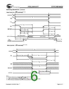
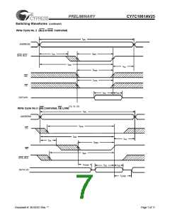
Write Cycle[8, 9]
tWC
Write Cycle Time
8
6
10
7
12
8
ns
ns
tSCE
CE1 LOW / CE2 HIGH to Write End
Notes:
3. Valid SRAM operation does not occur until the power supplies have reached the minimum operating VDD (2.3V). As soon as 1ms (Tpower) after reaching the
minimum operating VDD, normal SRAM operation can begin including reduction in VDD to the data retention (VCCDR, 1.5V) voltage.
4. Test conditions assume signal transition time of 3 ns or less, timing reference levels of 1.1V, input pulse levels of 0 to 2.5V, and output loading of the specified
IOL/IOH and specified transmission line loads. Test conditions for the Read cycle use output loading shown in part a) of the AC test loads, unless specified otherwise.
5. This part has a voltage regulator which steps down the voltage from 2.5V to 2V internally. tpower time has to be provided initially before a Read/Write operation
is started.
6. tHZOE, tHZCE, tHZWE, tHZBE and tLZOE, tLZCE, t\LZWE, tLZBE are specified with a load capacitance of 5 pF as in (b) of AC Test Loads. Transition is measured ±200 mV from
steady-state voltage.
7. These parameters are guaranteed by design and are not tested.
8. The internal Write time of the memory is defined by the overlap of CE1 LOW (CE2 HIGH) and WE LOW. Chip enables must be active and WE and byte enables must
be LOW to initiate a Write, and the transition of any of these signals can terminate the Write. The input data set-up and hold timing should be referenced to the leading edge of
the signal that terminates the Write.
9. The minimum Write cycle time for Write Cycle No. 3 (WE controlled, OE LOW) is the sum of tHZWE and tSD
.
Document #: 38-05331 Rev. **
Page 4 of 11

 CYPRESS [ CYPRESS ]