PRELIMINARY
CY7C1061AV25
DC Input Voltage[1] ................................ –0.5V to VCC + 0.5V
Maximum Ratings
(Above which the useful life may be impaired. For user guide-
lines, not tested.)
Current into Outputs (LOW)......................................... 20 mA
Operating Range
Storage Temperature .................................–65°C to +150°C
Ambient Temperature with
Power Applied.............................................–55°C to +125°C
Supply Voltage on VCC to Relative GND[1] .... –0.5V to +3.6V
Ambient
Range
Commercial
Industrial
Temperature
0°C to +70°C
–40°C to +85°C
VCC
2.5V ± 0.2V
DC Voltage Applied to Outputs
in High-Z State[1] ....................................–0.5V to VCC + 0.5V
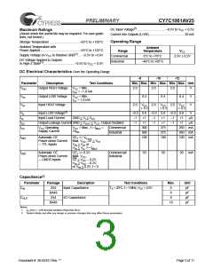
DC Electrical Characteristics Over the Operating Range
-8
-10
-12
Parameter
Description
Test Conditions
Min. Max. Min. Max. Min. Max. Unit
VOH
Output HIGH Voltage VCC = Min.,
2.0
2.0
2.0
V
V
V
IOH = –1.0 mA
VOL
VIH
Output LOW Voltage
Input HIGH Voltage
VCC = Min.,
IOL = 1.0 mA
0.4
0.4
0.4
2.0 VCC 2.0 VCC 2.0 VCC
+ 0.3 + 0.3 + 0.3
VIL
IIX
Input LOW Voltage[1]
Input Load Current
–0.3 0.8 –0.3 0.8 –0.3 0.8
V
GND < VI < VCC
–1
–1
+1
+1
–1
–1
+1
+1
–1
–1
+1
+1
µA
µA
IOZ
ICC
Output Leakage Current GND < VOUT < VCC, Output Disabled
VCC Operating
Supply Current
VCC = Max., f = fMAX
1/tRC
=
Commercial
Industrial
300
300
100
275
275
100
260 mA
260 mA
100 mA
ISB1
Automatic CE
CE2 <= VIL
Power-down Current
—TTL Inputs
Max. VCC, CE > VIH
VIN > VIH or
VIN < VIL, f = fMAX
ISB2
Automatic CE
Power-down Current
—CMOS Inputs
CE2 <= 0.2V
Max. VCC,
CE > VCC – 0.2V,
VIN > VCC – 0.2V,
or VIN < 0.2V, f = 0
Commercial/
Industrial
50
50
50
mA
Capacitance[2]
Parameter
Package
Z54
Description
Test Conditions
TA = 25°C, f = 1 MHz, VCC = 2.5V
Max.
6
Unit
CIN
Input Capacitance
pF
pF
pF
pF
BA48
Z54
8
COUT
I/O Capacitance
8
BA48
10
Notes:
1.
VIL (min.) = –2.0V for pulse durations of less than 20 ns.
2. Tested initially and after any design or process changes that may affect these parameters.
Document #: 38-05331 Rev. **
Page 3 of 11

 CYPRESS [ CYPRESS ]