BCM4330 Preliminary Data Sheet
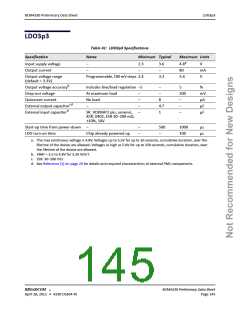
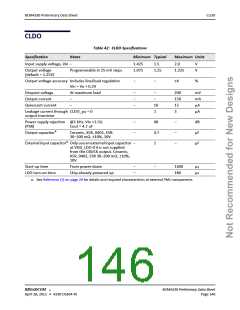
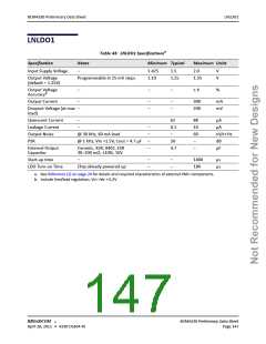
CLDO
CLDO
Table 42: CLDO Specifications
Minimum Typical
Specification
Notes
Maximum Units
Input supply voltage, Vin –
1.425
1.075
1.5
1.25
2.0
1.325
V
V
Output voltage
Programmable in 25 mV steps
(default = 1.25V)
Output voltage accuracy Includes line/load regulation
Vin > Vo + 0.2V
–
–
±4
%
Dropout voltage
Output current
Quiescent current
Leakage current through CLDO_pu = 0
output transistor
At maximum load
–
–
–
–
–
–
–
10
1
200
150
15
mV
mA
µA
3
µA
Power supply rejection @1 kHz, Vin >1.5V,
–
–
40
4.7
1
–
–
–
dB
µF
µF
(PSR)
Cout = 4.7 uF
a
Output capacitor
Ceramic, X5R, 0402, ESR:
30–200 mΩ, ±10%, 10V
a
External input capacitor Only use an external input capacitor –
at VDD_LDO if it is not supplied
from the CBUCK output. Ceramic,
X5R, 0402, ESR 30–200 mΩ, ±10%,
10V
Start-up time
LDO turn-on time
From power-down
Chip already powered up
–
–
–
1400
180
µs
µs
a. See Reference [1] on page 20 for details and required characteristics of external PMU components.
®
BROADCOM
BCM4330 Preliminary Data Sheet
April 28, 2011 • 4330-DS304-RI
Page 146

 CYPRESS [ CYPRESS ]