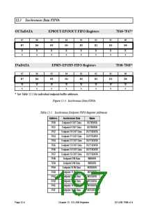
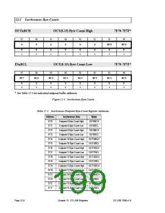
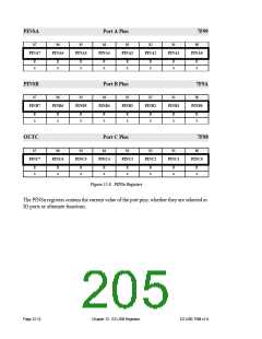
12.5 CPU Registers
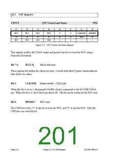
CPUCS
CPU Control and Status
7F92
b7
b6
b5
b4
b3
b2
b1
b0
RV3
RV2
RV1
RV0
0
0
CLK24OE
8051RES
R
R
R
R
R
0
R
0
R/W
1
R
1
RV3
RV2
RV1
RV0
Figure 12-5. CPU Control and Status Register
This register enables the CLK24 output and permits the host to reset the 8051 using a
Firmware Download.
Bit 7-4:
RV[3..0]
Silicon Revision
These register bits define the silicon revision. Consult individual Cypress Semiconductor
data sheets for values.
Bit 1:
CLK24OE Output enable - CLK24 pin
When this bit is set to 1, the internal 24-MHz clock is connected to the EZ-USB CLK24
pin. When this bit is 0, the CLK24 pin drives HI. This bit can be written by the 8051 only.
Bit 0:
8051RES
8051 reset
The USB host writes “1” to this bit to reset the 8051, and “0” to run the 8051. Only the
USB host can write this bit.
Page 12-8
Chapter 12. EZ-USB Registers
EZ-USB TRM v1.9

 CYPRESS [ CYPRESS ]