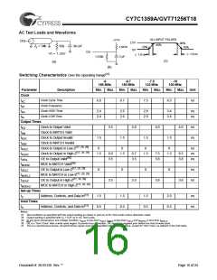
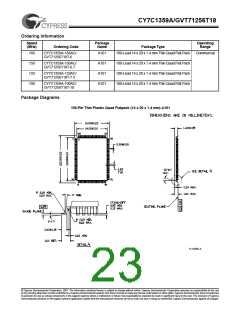
CY7C1359A/GVT71256T18
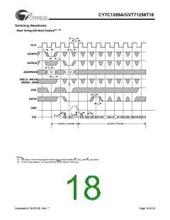
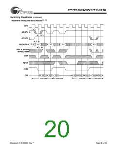
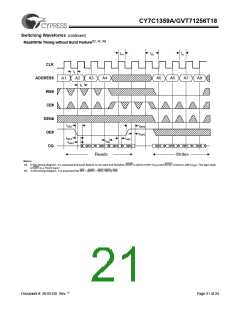
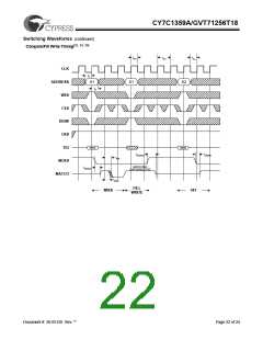
Switching Waveforms (continued)
Read/Write Timing without Burst Feature[32, 34, 35]
tKH
tKC
tKL
CLK
tS
ADDRESS
WE#
A2
A3
A4
A5
A6
A7
A8
A1
tH
CE#
DEN#
OE#
tOEQ
tOEHZ
tKQHZ
tOELZ
tKQLZ
tKQX
tKQ
Q(A1)
Q(A2)
Q(A3)
Q(A4)
D(A5)
D(A6)
D(A7)
D(A8)
DQ
Reads
Writes
Notes:
34. In this timing diagram, it is assumed that burst feature is not used and therefore ADSP is tied to HIGH (VCC) and ADSC is tied to LOW (VSS). The logic state
of ADV is a “Don’t Care”.
35. In this timing diagram, it is assumed that WE = [BWE + WEL*WEH]*GW.
Document #: 38-05120 Rev. **
Page 21 of 24

 CYPRESS [ CYPRESS ]