Bt8370/8375/8376
2.0 Circuit Description
2.8 Transmitter
Fully Integrated T1/E1 Framer and Line Interface
DL1 and DL2 are configured identically, except for their offset in the register
map. The DL1 address range is 0A4 to 0AE, and the DL2 address range is 0AF to
0B9. From this point on, the DL1 is used to describe the operation of both data
link controllers. Transmit Data Link 1 (TDL1) can be viewed as having a higher
priority than Transmit Data Link 2 (TDL2) because TDL1 overwrites the primary
rate channel after TDL2. Thus, any data that TDL2 writes to the primary rate
channel can be overwritten by TDL1, if TDL1 is configured to transmit in the
same time slot as TDL2.
The TDL1 is enabled using the DL1 Control register [DL1_CTL; addr 0A6].
TDL1 does not overwrite time slot data until it is enabled. DL1_CTL also
controls the data format and the circular buffer/FIFO mode.
The following data formats [DL1[1,0]; addr 0A6] are supported on the data
link: Frame Check Sequence (FCS), non-FCS, Pack8, or Pack6. FCS and
non-FCS are HDLC-formatted messages. Pack8 and Pack6 are unformatted
messages with 8 bits per FIFO access, and 6 bits per FIFO access, respectively.
The Circular Buffer/FIFO control bit [TDL1_RPT; addr 0A6] allows the FIFO
to act as a circular buffer; in this mode, a message can be transmitted repeatedly.
This feature is available only for unformatted transmit data link applications. The
processor can repeatedly send fixed patterns on the selected channel by writing a
1- to 64- byte message into the circular buffer. The programmed message length
repeats until the processor writes a new message. The first byte of each
unformatted message is output automatically, aligned to the first frame of the 12-,
24-, or 16-frame transmit multiframe (SF/ESF/MFAS). This allows the processor
to source overhead or data elements aligned to the TX timebase.
NOTE: Each unformatted message written is output-aligned only after the
preceding message completes transmission. Therefore, data continuity is
retained during the linkage of consecutive messages, provided that the
contents of each message consists of a multiple of the multiframe length.
Time slot and bit selection is done through the DL1 Time Slot Enable
[DL1_TS; addr 0A4] and DL1 Bit Enable [DL1_BIT; addr 0A5] registers.
DL1_TS selects which frames and which time slot are overwritten. The frame
select allows TDL1 to overwrite the time slot in all frames, odd frames, even
frames. The time slot word enable is a value between 0 and 31 that selects which
time slot is filled with data from the transmit data link buffer. DL1_BIT selects
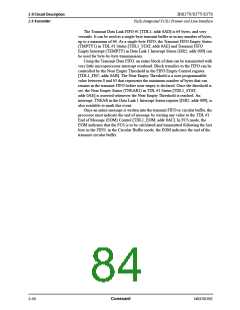
which bits are overwritten in the time slot selected. Table 2-10 lists commonly
used data link settings.
Table 2-10. Commonly Used Data Link Settings
Time Slot
Data Link
Frame
Time Slot
Mode
Bits
ESF FDL
T1DM R Bit
SLC-96
Odd
All
0 (F-bits)
Don’t Care
00000010
Don’t Care
11111111
00001000
FCS
FCS
24
Even
All
0 (F-bits)
Pack6
FCS
ISDN LAPD
CEPT Sa4
N
1
Odd
FCS
NOTE(S): N represents any T1/E1 time slot.
N8370DSE
Conexant
2-55

 CONEXANT [ CONEXANT SYSTEMS, INC ]